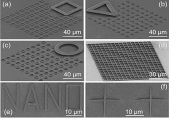
Laser etching technology has become indispensable in the precision processing of thin-film materials, particularly in industries such as display manufacturing, photovoltaics, and flexible electronics. Despite its advantages in non-contact processing, digital control, and high precision, several technical challenges persist in the development and application of thin-film laser etching equipment. This article explores these challenges and the innovative solutions driving the industry forward.
With the continuous innovation of MEMS technology, MEMS devices are widely used in consumer electronics, medical equipment, and aerospace applications, offering significant value due to their compact size, high speed, reliability, and low cost. MEMS packaging is a critical step in MEMS device development.
The manufacturing process of perovskite solar cells involves multiple precise steps, with laser technology playing a critical role in enhancing efficiency and stability. The key steps include:
Substrate Preparation: Cleaning and pre-treating the substrate (e.g., glass or flexible polymers) to ensure optimal adhesion and conductivity.
Electrode Deposition: Depositing transparent conductive oxides (e.g., ITO or FTO) as bottom electrodes.
Perovskite solar cells (PSCs) represent a transformative technology in photovoltaics, with industrialization accelerating globally. Unlike traditional silicon-based cells, PSCs require entirely new production processes and equipment, creating significant investment opportunities in specialized manufacturing tools. The core equipment includes coating, deposition, laser, and encapsulation systems, with laser etching and thin-film deposition being particularly critical for scalable production.


 Cell Laser Scribing Machine")


 Co., Ltd.")