Cell Laser Scribing Machine")


 Co., Ltd.")
Investment Opportunities in Perovskite Solar Cell Industrialization: Key Equipment and Laser Processes
Perovskite solar cells (PSCs) represent a transformative technology in photovoltaics, with industrialization accelerating globally. Unlike traditional silicon-based cells, PSCs require entirely new production processes and equipment, creating significant investment opportunities in specialized manufacturing tools. The core equipment includes coating, deposition, laser, and encapsulation systems, with laser etching and thin-film deposition being particularly critical for scalable production.
1. Key Equipment for Perovskite Production Lines
The unique layered structure of PSCs—stacking functional films including the hole transport layer (HTL), perovskite layer, and electron transport layer (ETL)—demands precise and scalable fabrication techniques. The following equipment categories are essential:
Deposition Equipment (PVD/RPD): Used for HTL and ETL layers. Physical Vapor Deposition (PVD) techniques include thermal evaporation, sputtering, and ion plating(RPD). These processes form uniform, high-quality films but require high capital investment.
Coating Equipment: Primarily slot-die coatersfor depositing the perovskite light-absorbing layer. This wet process offers cost efficiency and high material utilization but challenges in thickness uniformity.
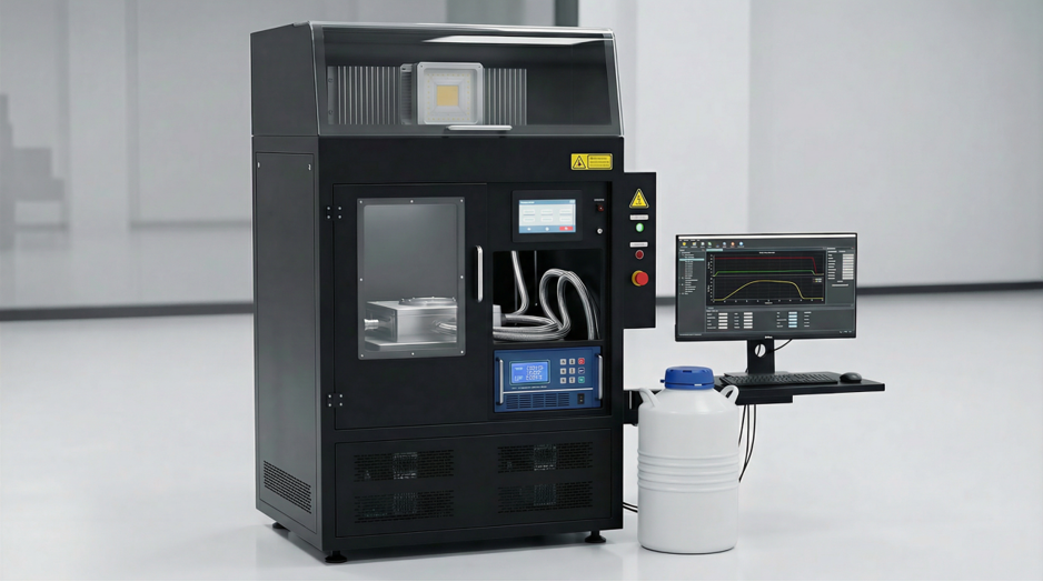
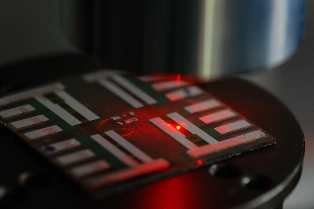
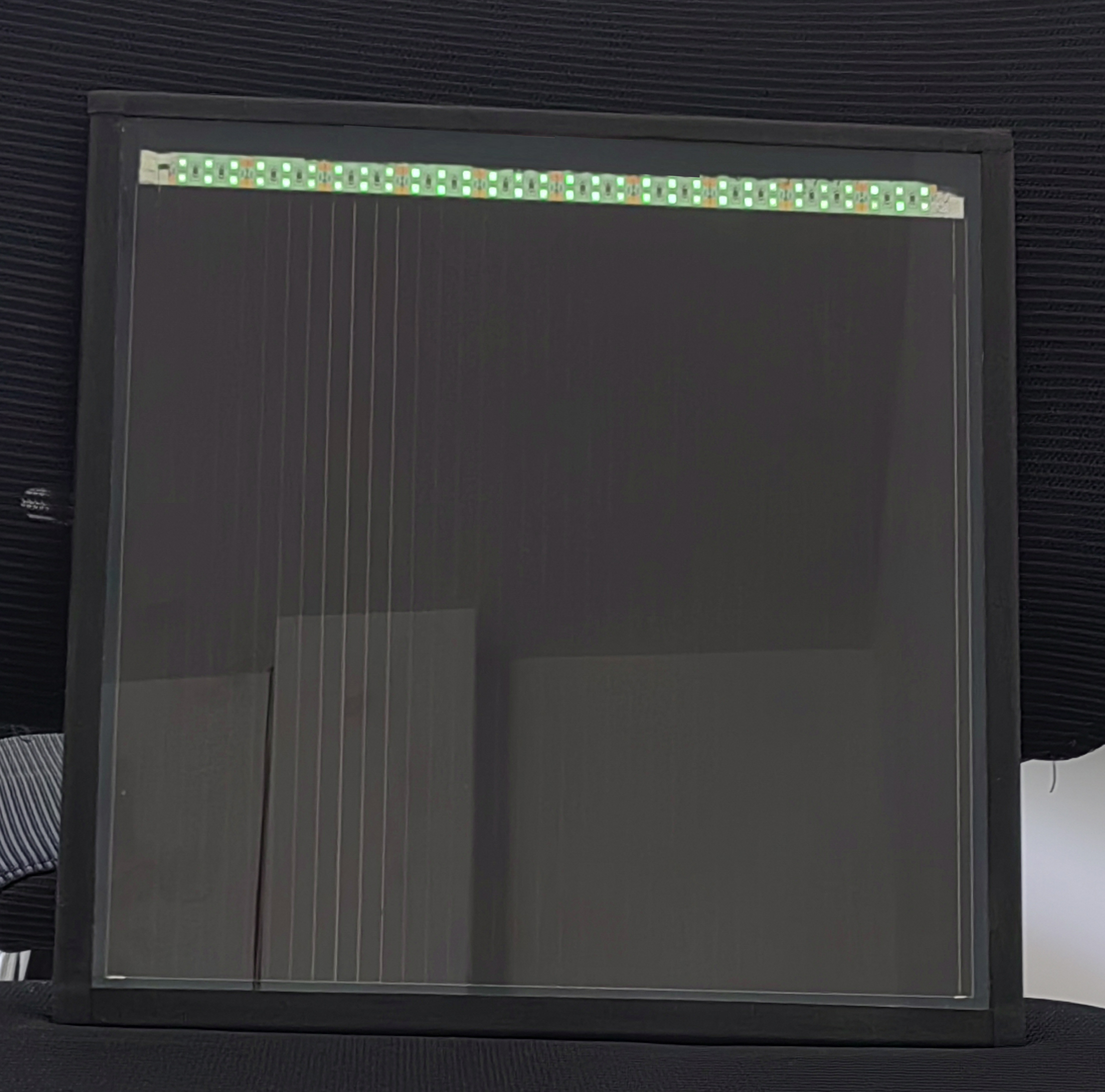
Laser Equipment: Indispensable for patterning and interconnecting cell modules. Laser systems perform critical etching steps (P1–P4) to define cell boundaries and ensure series connection.
Encapsulation Systems: Protect moisture-sensitive perovskite layers from degradation, ensuring long-term stability.
2. Laser Etching: The Core of Perovskite Patterning
Laser processes are integral to PSC manufacturing, enabling precise patterning for series interconnection and performance optimization. The four laser steps include:
P1 Etching: After transparent conductive oxide (TCO) deposition, isolates individual electrode strips.
P2 Etching: Removes HTL/perovskite/ETL stacks to create voids filled by back electrodes, connecting adjacent cells.
P3 Etching: Separates adjacent cells by removing electrode/HTL/perovskite/ETL stacks, leaving TCO intact.
P4 Edge Isolation: Clears peripheral areas for encapsulation.
These steps ensure minimal electrical losses and high module efficiency.

3. Perovskite Layer Deposition: Coating vs. Vapor Methods
The perovskite layer deposition is pivotal for cell performance. Large-area techniques include:
Slot-Die Coating: Dominates for its scalability, continuous production capability, and >90% material utilization. However, it requires high-precision equipment to control uniformity.
Blade Coating: Low-cost but suffers from material waste.
Spray/Inkjet Printing: Suitable for flexible substrates but limited by low efficiency and maintenance complexity.
Vapor Deposition: Offers superior film quality and uniformity but has low material utilization and throughput.
Industry players like GCL Optoelectronicsuse slot-die coating in 100MW pilot lines, while others explore vapor-phase methods for premium applications.

4. Deposition Techniques for Transport Layers
HTL and ETL layers rely on dry processes like PVD:
Thermal Evaporation: High purity and maturity but moderate adhesion.
Sputtering: Excellent thickness control and adhesion but prone to edge thinning.
Ion Plating (RPD): Superior film quality with minimal damage to underlying layers, though target utilization is suboptimal.
5. Comparative Analysis: Wet vs. Dry Processes
The choice between coating (wet) and PVD (dry) involves trade-offs:
Coating (Wet): Lower cost, high material efficiency, but uneven thickness.
PVD (Dry): Excellent uniformity and reproducibility but high equipment costs.
Companies like Jingshan Light Machineryand Jiejia Weichuangprovide hybrid solutions to balance these factors.
6. Industrialization Status and Outlook
China leads in perovskite industrialization, with GW-scale production lines operational (e.g., Jedi Light Energyin Wuxi). Policies in Shandong, Guangdong, and Jiangsu provinces support equipment localization and demonstration projects. By 2027, the cost of perovskite modules is expected to drop below $0.06/W, driven by improved equipment efficiency and scale.
Conclusion
Perovskite solar cell industrialization hinges on advanced equipment, particularly laser and deposition systems. Laser etching ensures precision patterning, while coating and PVD technologies enable scalable thin-film deposition. With global capacity expanding, investments in high-precision, automated equipment will define the next phase of perovskite commercialization.