


40px
80px
80px
80px
Lecheng Intelligent Technology Suzhou
Phone
+86-17751173582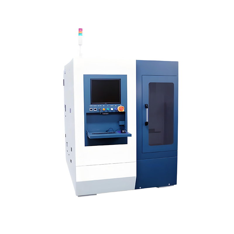
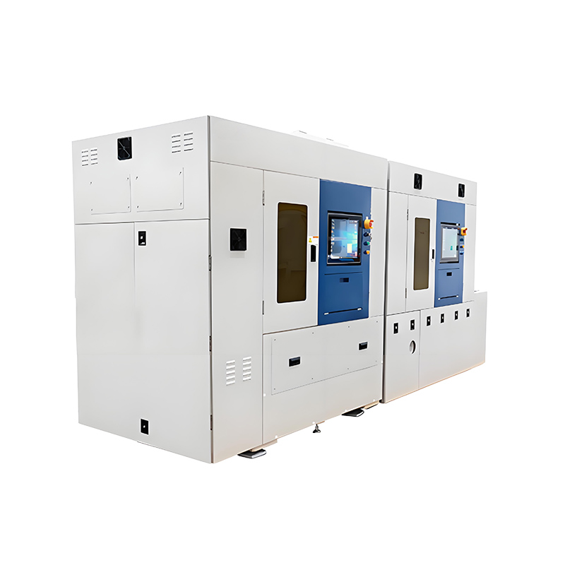
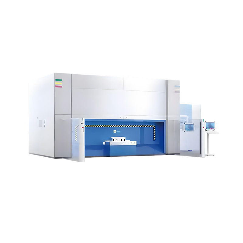
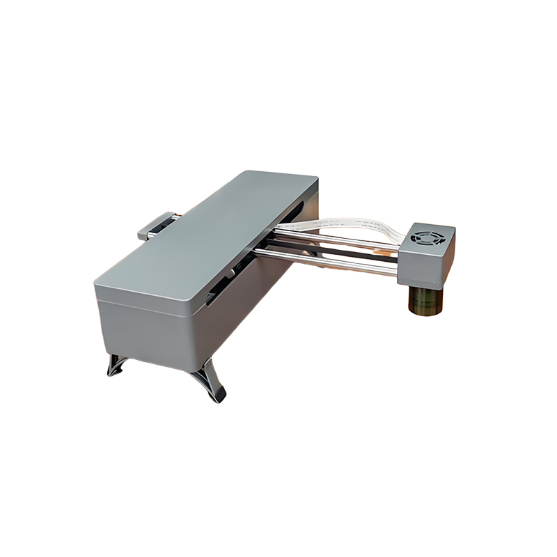
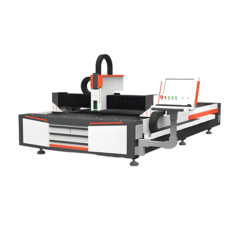
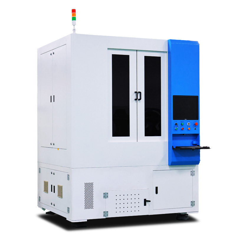
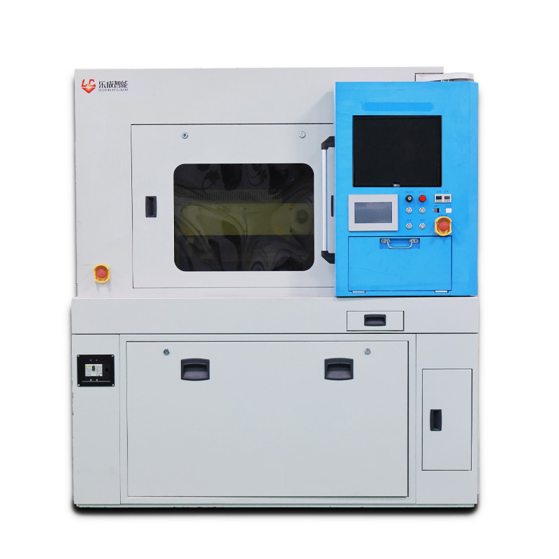
Silicon Carbide Ingot Laser Slicing System is designed for industrial laser processing projects that require stable beam control, process repeatability, and reliable integration with production requirements. For ├ Laser Cutting Equipment selection, buyers should compare material type, processing accuracy, automation level, throughput, maintenance access, and after-sales support before confirming the final equipment configuration.
Related laser solutions include Flexible OLED Laser Cutting System, 3D Laser Cutting Machine, P-Series High-Speed Laser Tube Cutting Machine. These internal references help users compare similar systems and move naturally between cleaning, cutting, scribing, marking, welding, and photovoltaic laser equipment pages.
High-Power Ultrafast Laser System: Utilizes picosecond/femtosecond pulsed lasers to minimize heat-affected zones (HAZ) and material damage.
Precision Motion Stage: Equipped with linear motor-driven systems, achieving ±1μm repeat positioning accuracy for stable and consistent cutting paths.
Adaptive Optical Focusing: Dynamically adjusts laser focal points to accommodate ingots of varying thicknesses, ensuring optimal cutting quality.
Real-Time Monitoring & Feedback: Integrated CCD vision alignment and laser ranging systems enable live process control with automatic parameter adjustment.
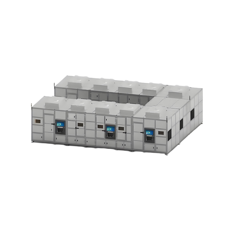
Modular Design: Supports multi-station configurations, compatible with 4-inch, 6-inch, and 8-inch ingots for enhanced flexibility.

Low Material Waste: Non-contact laser cutting achieves kerf widths of 20–50μm, improving material yield by over 30%.
High Throughput: 5–10× faster than diamond wire saws, reducing processing time to <2 hours per ingot.
Superior Surface Quality: Cut surface roughness (Ra) <0.5μm, minimizing post-polishing steps and costs.
Eco-Friendly: Eliminates cutting fluid pollution and reduces energy consumption by 40%, aligning with sustainable manufacturing.

SiC Power Devices: Ideal for wafer preparation of MOSFETs, SBDs, and other power electronics.
RF Components: Enables precise slicing for GaN-on-SiC wafers in 5G base stations and satellite communication systems.
New Energy Vehicles: Supports SiC wafer production for EV inverters, OBC modules, and other critical components.

40px
80px
80px
80px
Lecheng Intelligent Technology Suzhou
Phone
+86-17751173582