


40px
80px
80px
80px
Lecheng Intelligent Technology Suzhou
Phone
+86-17751173582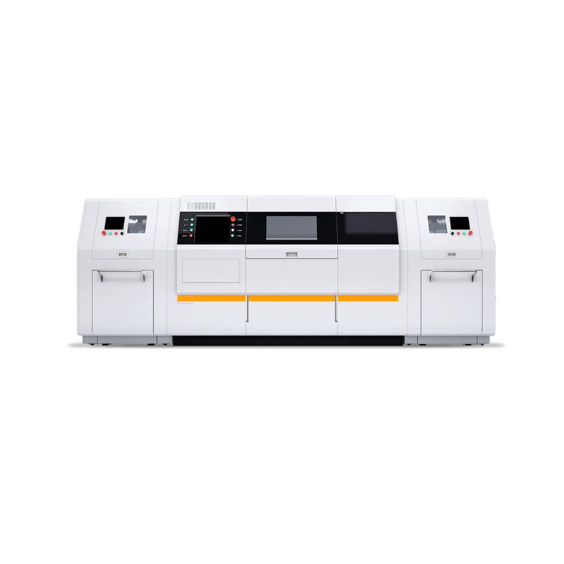
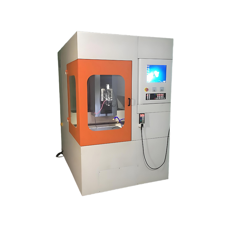
Consumer Electronics Laser Drilling Equipment is designed for industrial laser processing projects that require stable beam control, process repeatability, and reliable integration with production requirements. For ├ Laser Integrated Processing selection, buyers should compare material type, processing accuracy, automation level, throughput, maintenance access, and after-sales support before confirming the final equipment configuration.
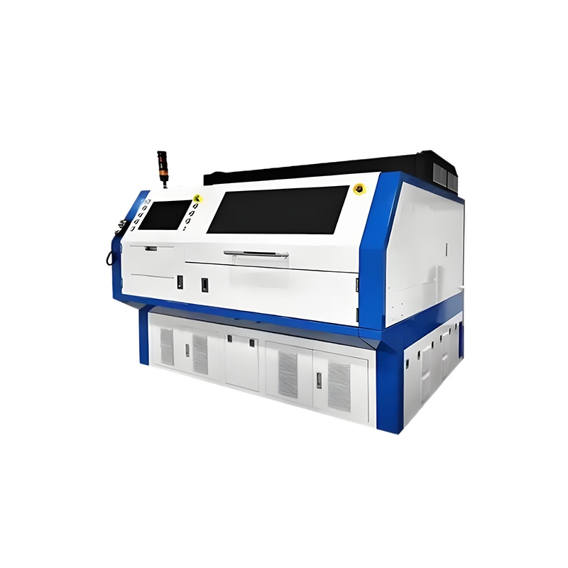
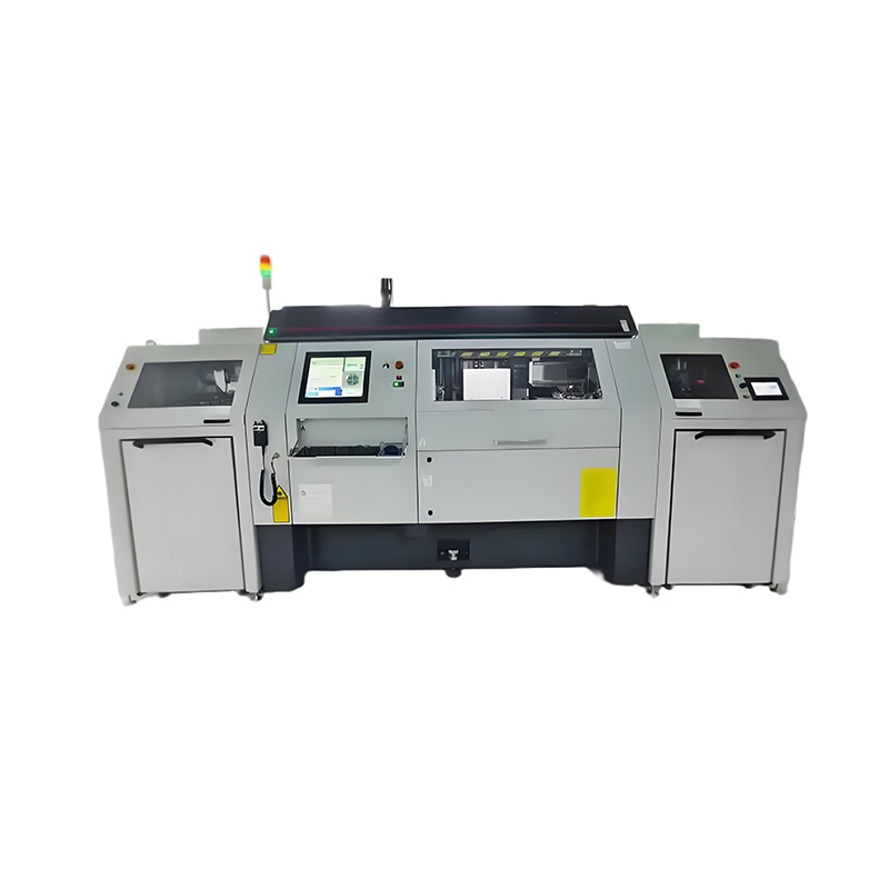
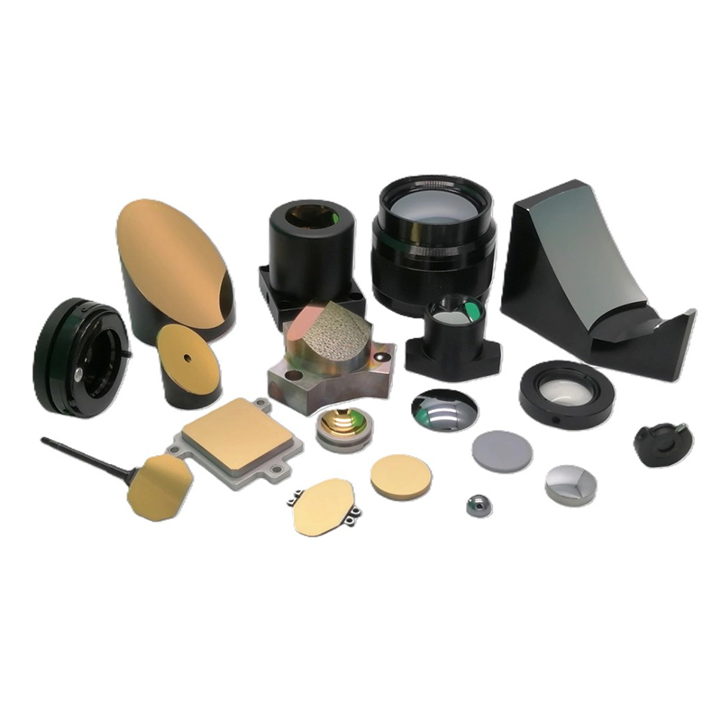
Related laser solutions include PCB Drilling Equipment, HDI Microvia Drilling Equipment, Laser Optics and Accessories. These internal references help users compare similar systems and move naturally between cleaning, cutting, scribing, marking, welding, and photovoltaic laser equipment pages.
Overview
Precision laser drilling system designed for smartphones, tablets and wearables. Utilizing UV laser technology, it achieves ±5μm accuracy on 0.05mm micro-vias across FR4, ceramic, FPC and glass substrates, meeting demands for miniaturized electronics manufacturing.

Feature | Performance | Value Proposition |
|---|---|---|
Ultra-Precision | ±5μm positioning | 99.98% yield rate |
High-Speed | 500 holes/sec | 3x productivity gain |
Smart Control | AI thermal compensation | 30% scrap reduction |
Multi-Material | FR4/Ceramic/FPC/Glass | <2min changeover |
Non-Contact:No mechanical stress damage
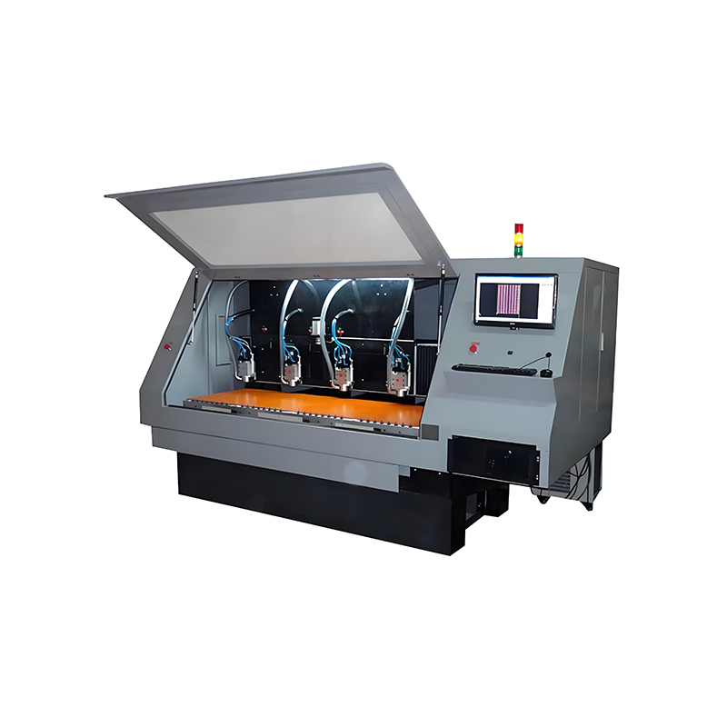
Micro-Drilling:0.05-0.3mm hole arrays
Eco-Friendly:70% energy saving, <65dB noise
Smartphones:HDI micro-vias/Camera alignment
TWS Earbuds:FPC irregular holes/Charging ports
Smartwatches:AMOLED display circuit vias
40px
80px
80px
80px
Lecheng Intelligent Technology Suzhou
Phone
+86-17751173582