


40px
80px
80px
80px
Lecheng Intelligent Technology Suzhou
Phone
+86-17751173582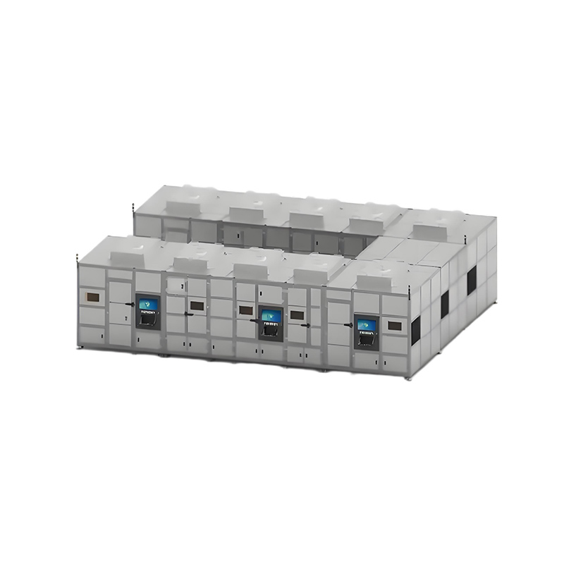
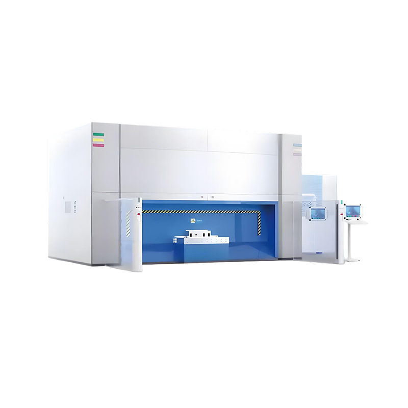
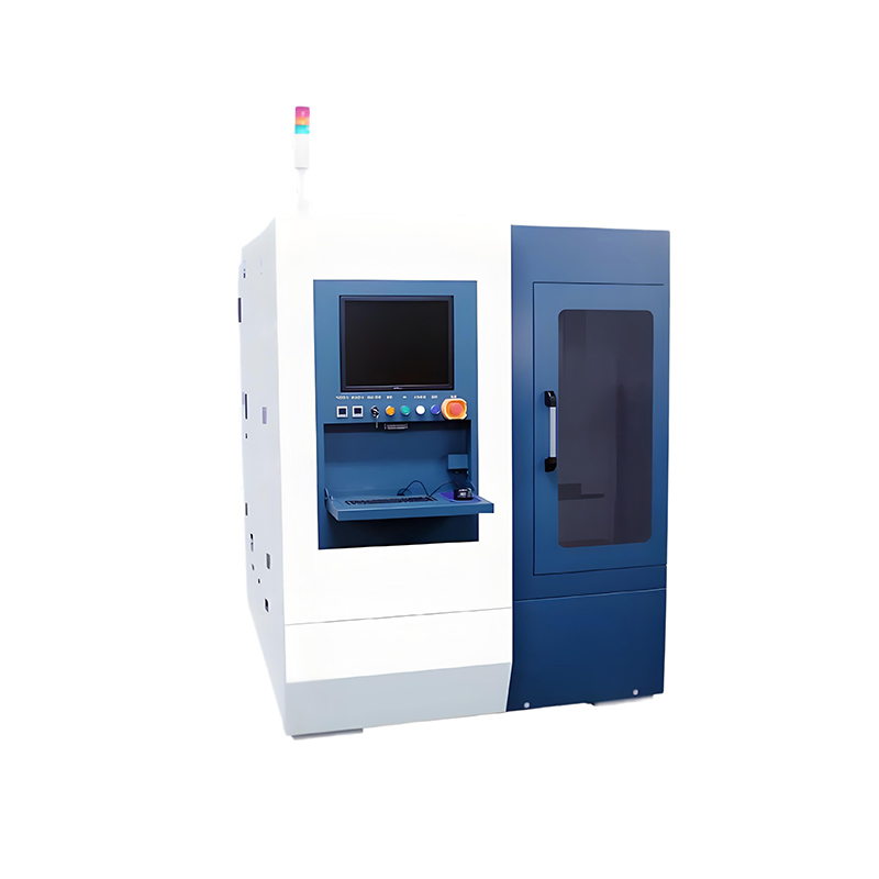
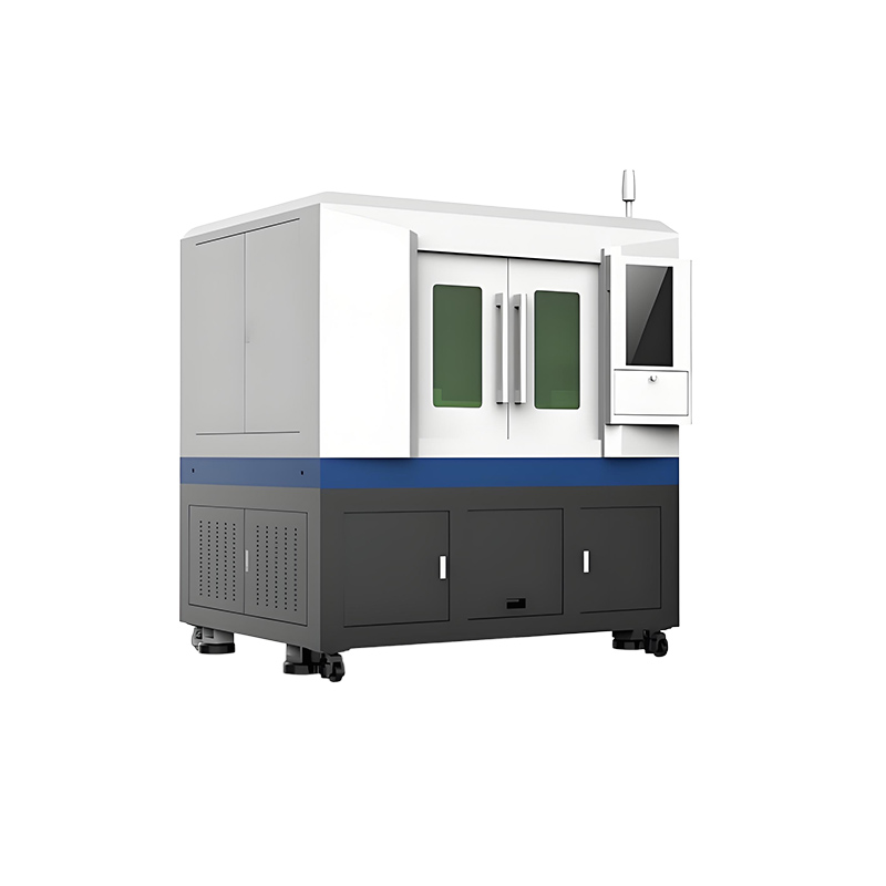
Flexible OLED Laser Cutting System is designed for industrial laser processing projects that require stable beam control, process repeatability, and reliable integration with production requirements. For ├ Laser Cutting Equipment selection, buyers should compare material type, processing accuracy, automation level, throughput, maintenance access, and after-sales support before confirming the final equipment configuration.
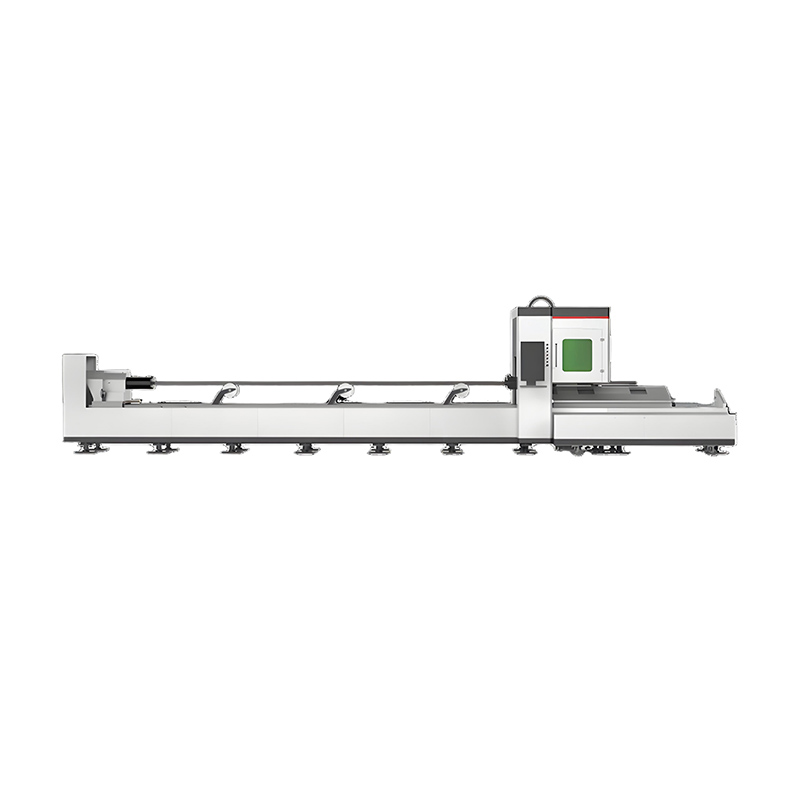
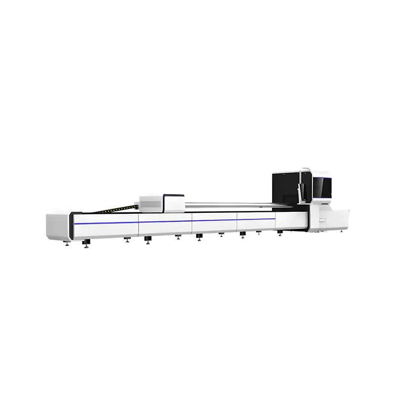
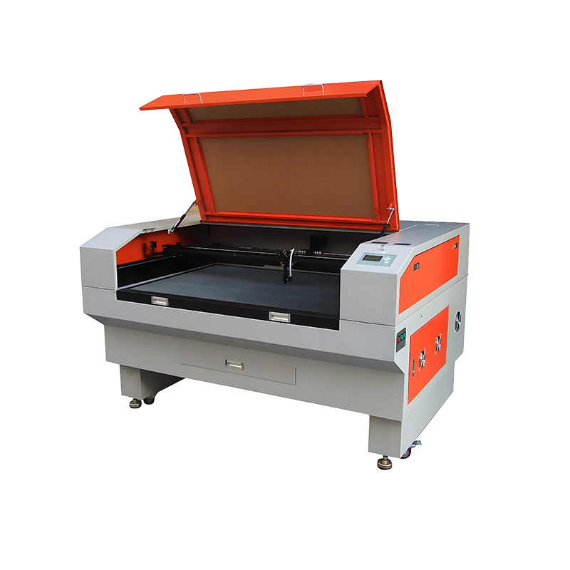
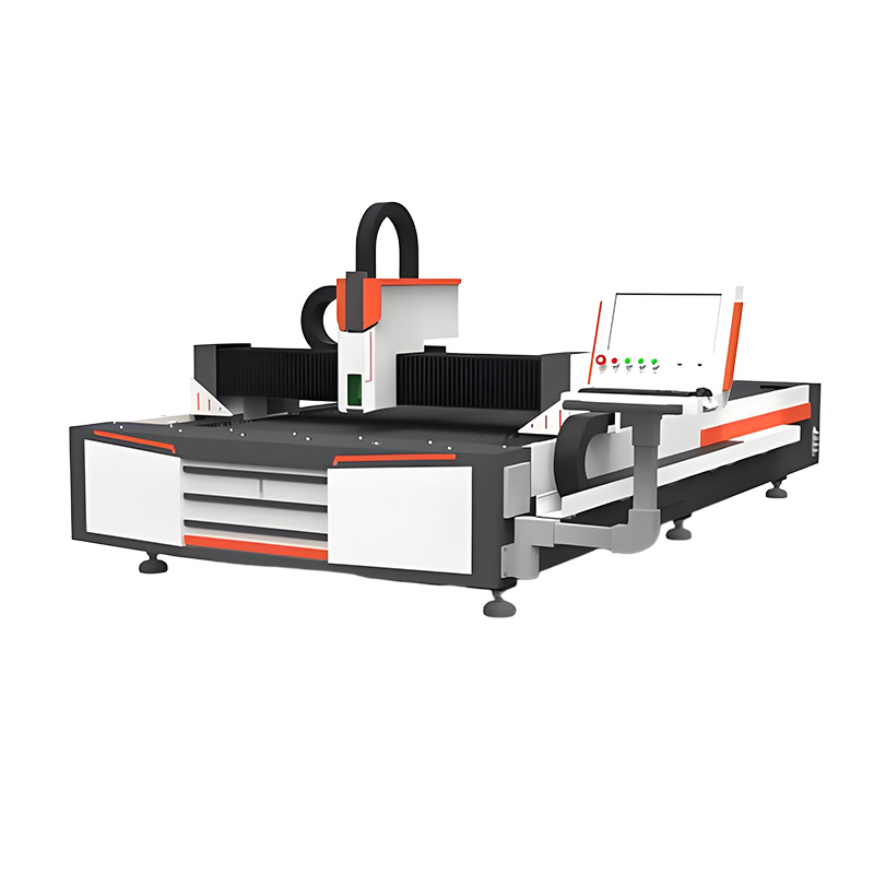
Related laser solutions include 3D Laser Cutting Machine, P-Series High-Speed Laser Tube Cutting Machine, Dual-Chuck Laser Tube Cutting Machine. These internal references help users compare similar systems and move naturally between cleaning, cutting, scribing, marking, welding, and photovoltaic laser equipment pages.
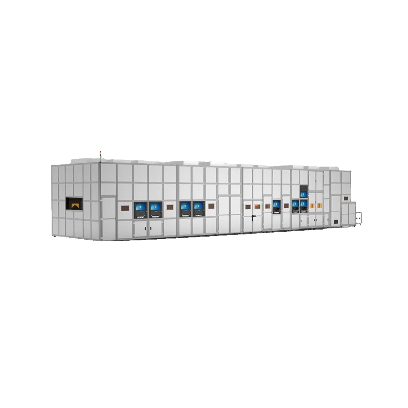
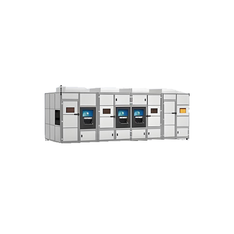
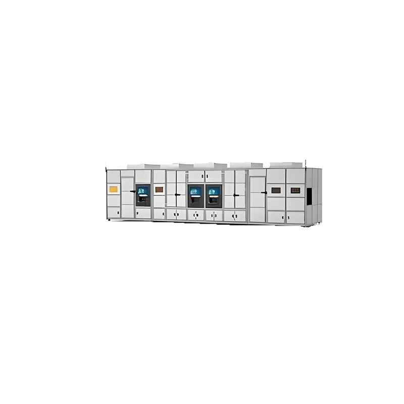
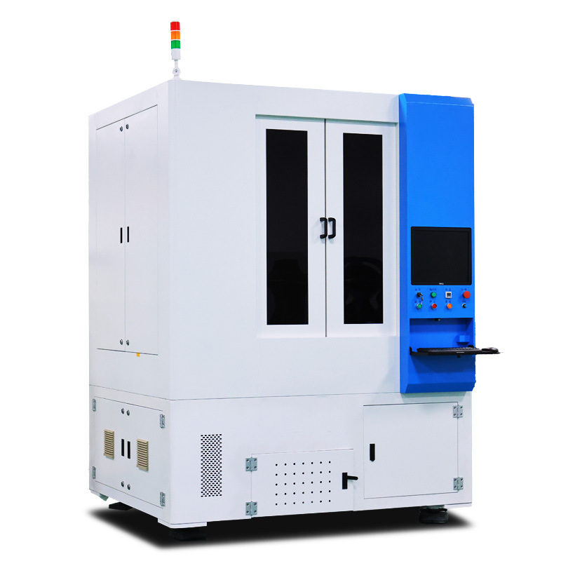
The Flexible OLED Laser Cutting System is a high-precision processing equipment specifically designed for flexible OLED display panels. Utilizing advanced UV ultrafast laser technology combined with precision motion control and intelligent vision systems, it delivers exceptional cutting quality for next-generation flexible displays, particularly suitable for foldable phones and curved display applications.

Laser System:
355nm UV picosecond laser source
<10ps pulse width, >10kW peak power
Adjustable repetition rate (100kHz-2MHz)
Motion System:
High-precision linear motor stages
±3μm positioning accuracy, ±1μm repeatability
Maximum speed of 500mm/s
Vision System:
5MP high-resolution CCD camera
±1μm auto-focus accuracy
Mark recognition and auto-compensation
Control System:
Industrial PC-based control platform
Direct CAD file import
Automatic cutting path optimization
Specification | Parameter | Benefit |
|---|---|---|
Cutting Accuracy | ±3μm | Flawless edge quality |
Edge Roughness | Ra<0.1μm | No post-polishing needed |
Processing Speed | 300mm/s | High production throughput |
Minimum Kerf Width | 20μm | Supports high-density designs |
Power Consumption | <5kW | 40% lower operating costs |
Key Advantages:
Non-contact processing eliminates mechanical stress
<5μm heat-affected zone protects OLED layers
Supports complex contour cutting
High automation with user-friendly operation
Foldable Devices:
Smartphone foldable displays
Tablet flexible screens
Wearables:
Smartwatch circular displays
AR/VR curved screens
Automotive Displays:
Center console curved panels
Instrument cluster displays
TV Applications:
Large-size OLED TV panels
Ultra-thin flexible modules
40px
80px
80px
80px
Lecheng Intelligent Technology Suzhou
Phone
+86-17751173582