The Application of Laser Technology in the Industrialization of Perovskite Solar Cells
Perovskite solar cells (PSCs) represent the third generation of thin-film solar technology, renowned for their high efficiency, low cost, and flexibility. As industrialization progresses, laser technology has emerged as a critical enabler, addressing key challenges in precision processing and scalability. This article explores the multifaceted role of lasers in PSC manufacturing.
1. Laser Processing in PSC Manufacturing
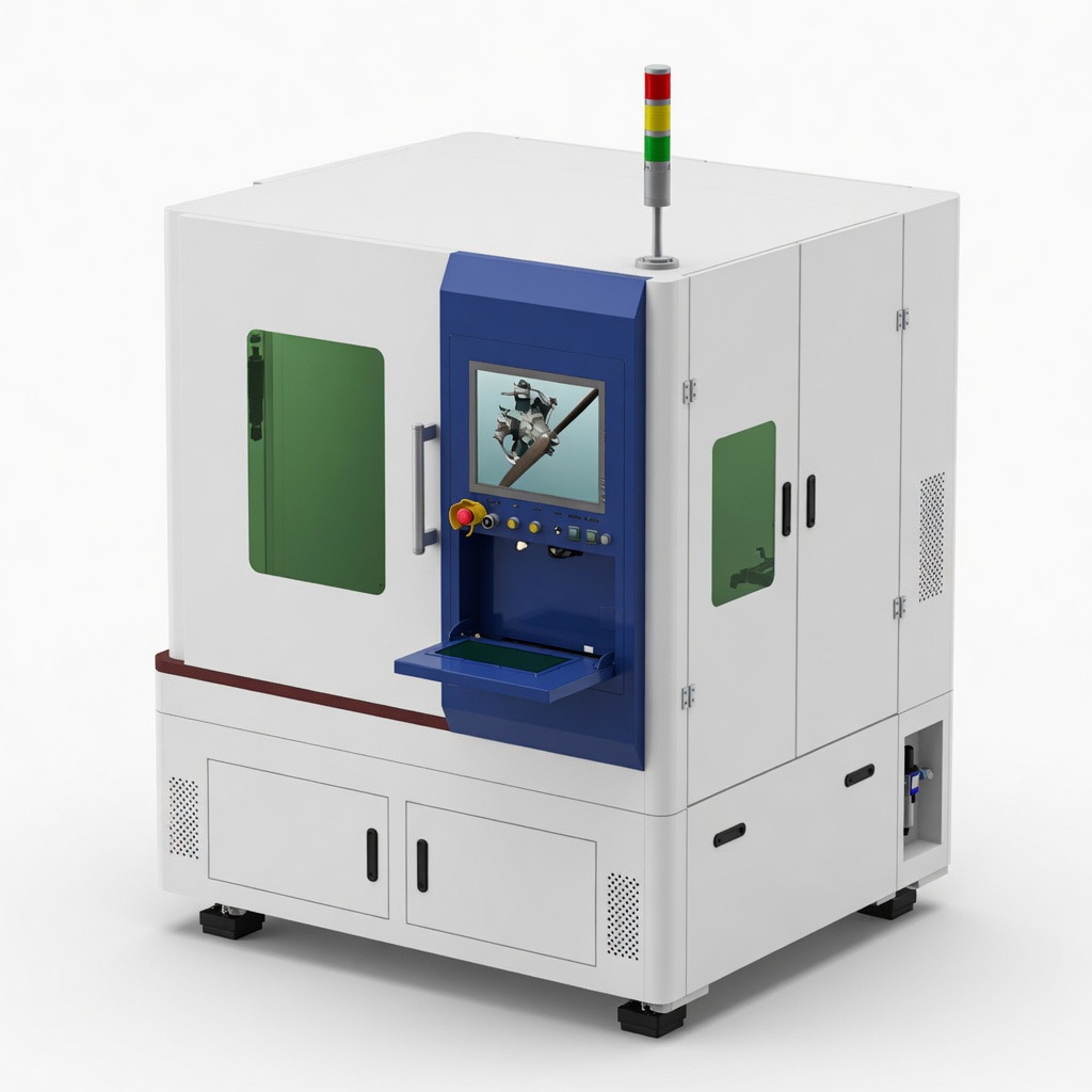
The production of perovskite solar cells involves four essential laser-based steps, designated as P1, P2, P3, and P4:
P1 Laser Patterning: After depositing the transparent conductive oxide (TCO) layer, lasers create isolated strips to define individual electrode regions. This step requires high precision to avoid damaging underlying layers.
P2 Laser Etching: Following the deposition of the hole transport layer (HTL), perovskite layer, and electron transport layer (ETL), lasers remove these layers to expose the TCO. This allows the back electrode to connect adjacent sub-cells, forming a series circuit.
P3 Laser Etching: Lasers remove the back electrode, HTL, perovskite, and ETL layers to isolate individual cells, preventing electrical shortcuts and ensuring efficient current collection.
P4 Edge Cleaning: Lasers clear a 10 mm-wide region along the glass edges to create an insulation zone for encapsulation, critical for long-term stability.
These steps demand precision within 0.3–0.5 μm, surpassing requirements for silicon cells, and rely on ultrafast lasers (e.g., femtosecond or picosecond lasers) to minimize thermal damage.
2. Advantages of Laser Technology
Laser processing offers distinct benefits over traditional methods:
Precision and Flexibility: Ultrafast lasers enable "cold processing," reducing heat-induced defects and enabling fine patterning on rigid or flexible substrates.
Efficiency Enhancement: By minimizing dead zones and ensuring clean edges, lasers boost cell efficiency. Studies show laser-treated PSCs achieve higher fill factors and reduced carrier recombination.
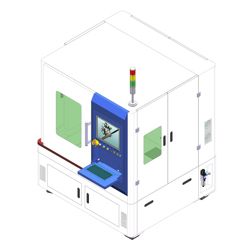
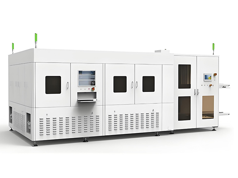
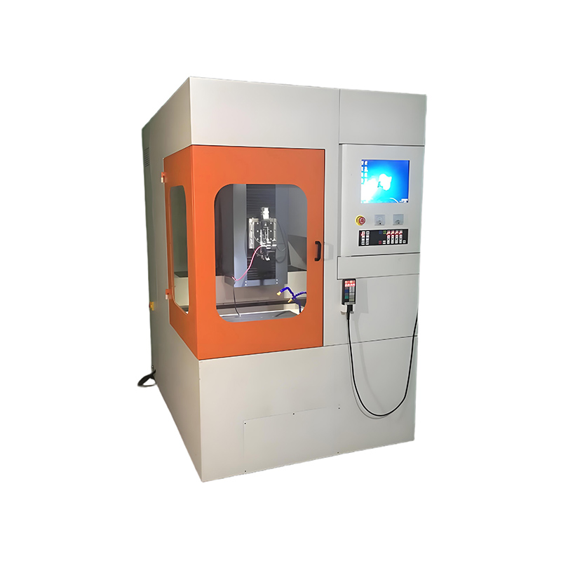
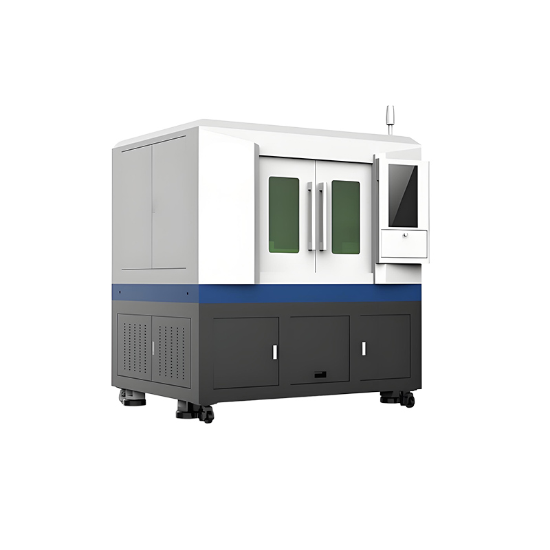
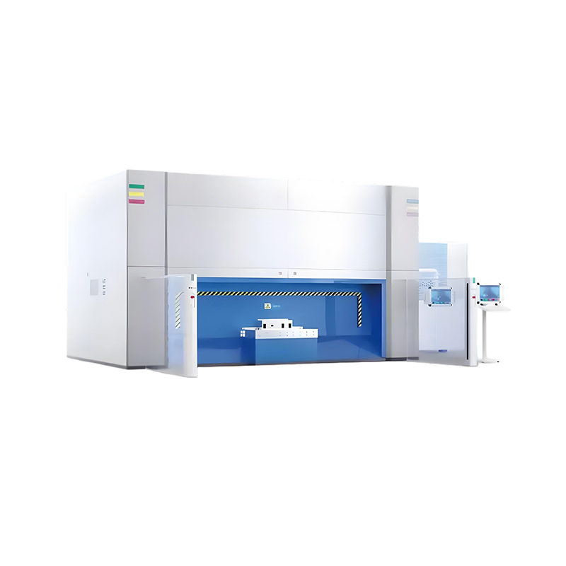
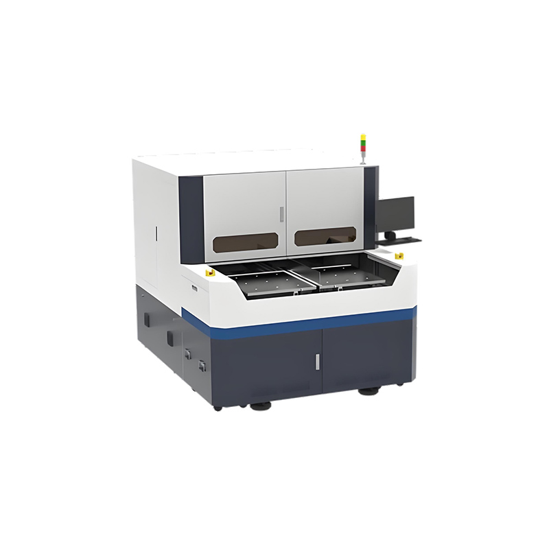
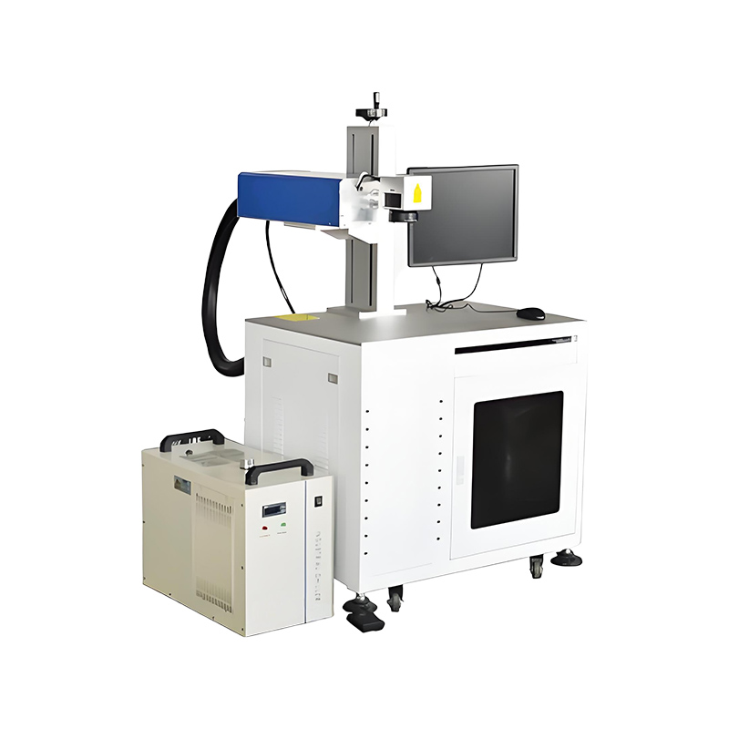
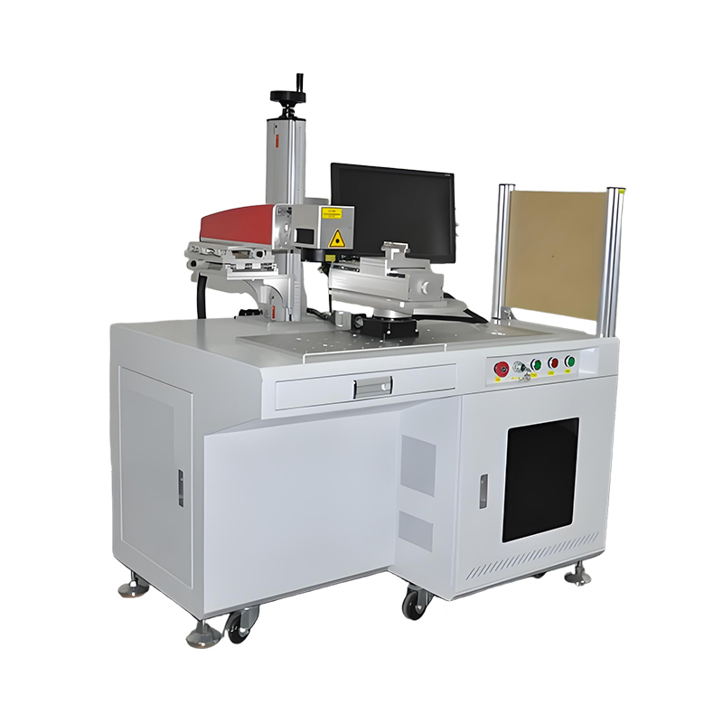
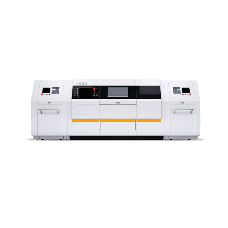
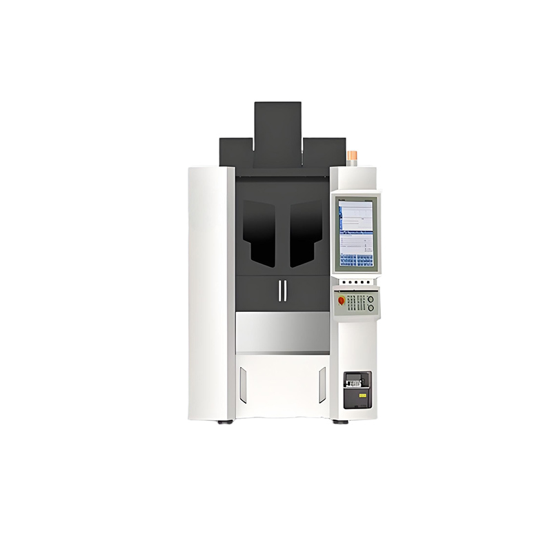
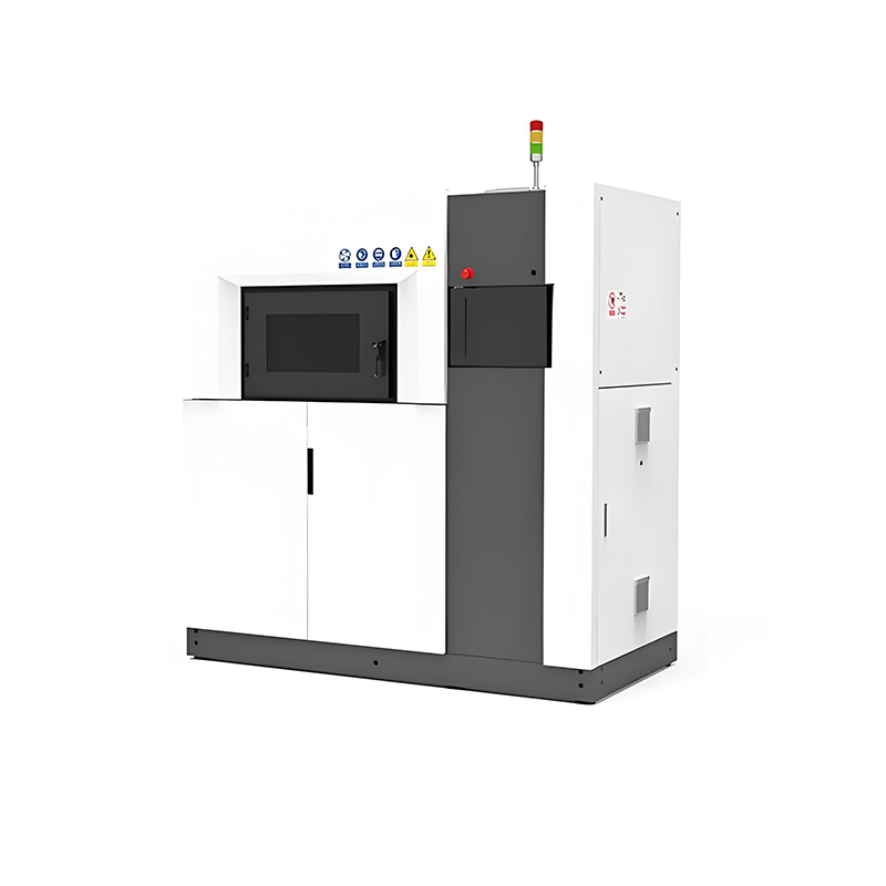
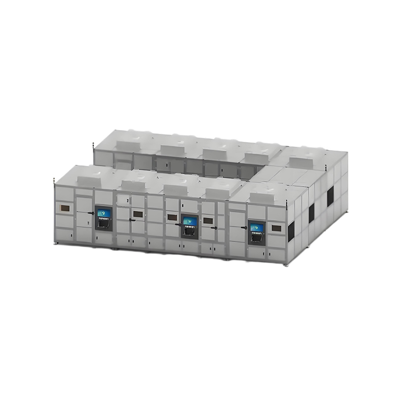
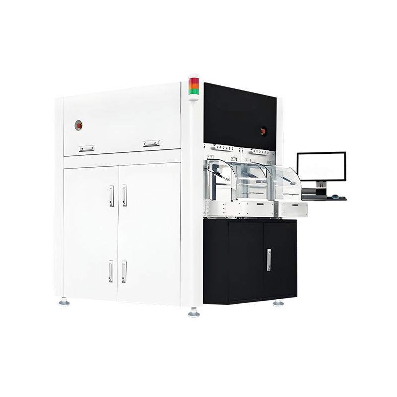
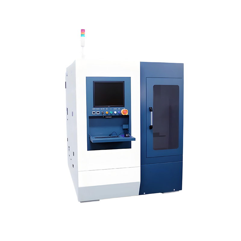
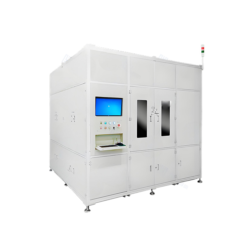
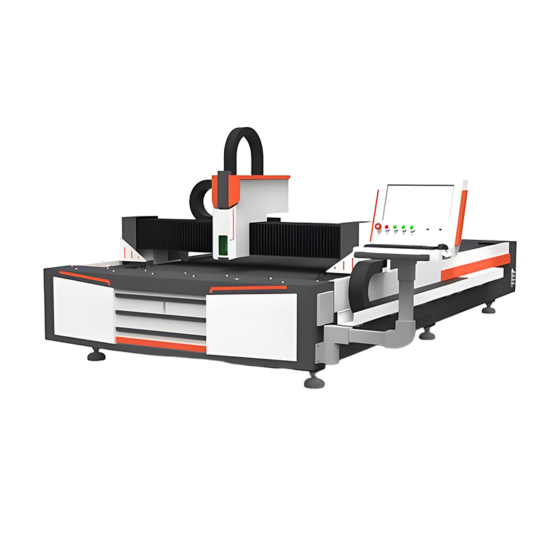
Scalability: Laser systems like Qingdao Zima’s femtosecond equipment support large-area processing (e.g., 1200 × 2400 mm panels), which is vital for GW-scale production.
3. Technological Innovations
Recent advances focus on improving laser techniques and integration:
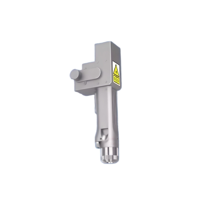
Beam Shaping: Converting Gaussian beams into flat-top beams ensures uniform energy distribution, reducing edge damage.
Dynamic Tracking: Real-time visual compensation and focus-following systems adjust laser paths to account for substrate deformations, maintaining consistency across large panels.
Excimer Laser Applications: KrF (248 nm) and XeCl (308 nm) lasers enhance film quality and enable low-temperature processing for flexible PSCs.
4. Challenges and Future Outlook
Despite progress, challenges remain:
Stability: Laser-induced defects can accelerate degradation, requiring finer control of parameters.
Cost Reduction: While laser equipment accounts for ~16% of production line costs, scaling to GW levels could lower expenses through modular design and higher throughput.
The market for PSC laser equipment is projected to exceed ¥8 billion in China by 2030, driven by产能 expansion
. Companies like DeLong Laser, JPT, and Lead Intelligent are pioneering integrated solutions to support this growth.
Conclusion
Laser technology is indispensable to the industrialization of perovskite solar cells, enabling precision patterning, efficiency gains, and large-scale production. Ongoing innovations in beam control and dynamic tracking will further solidify its role in achieving low-cost, high-efficiency photovoltaic solutions.

