How long does it take from equipment ordering to official production when cooperating with Locsen?
The overall timeline varies depending on equipment specifications and production line scale. For standalone equipment, standard models require a 45-day manufacturing cycle, with total duration (including shipping and installation) of approximately 60 days. Customized equipment requires an additional 30 days based on technical requirements.
For complete line solutions:
• 100MW-level production lines require ~4 months for planning, equipment manufacturing, installation, and commissioning
• GW-level production lines require ~8 months
We provide detailed project schedules with dedicated managers ensuring seamless coordination. Example: A client's 1GW perovskite production line was completed 15 days ahead of schedule through parallel equipment manufacturing and facility construction.
Does Locsen offer suitable equipment and partnership solutions for startup perovskite companies
Locsen offers a "Phased Partnership Program" specifically designed for perovskite startups.
For the initial R&D phase, we provide compact pilot-scale equipment (e.g., 10MW laser scribing systems) bundled with essential process packages to facilitate technology validation and product iteration.
During scale-up phases, startups qualify for upgrade benefits:
• Core modules from pilot equipment can be traded in with value deduction toward production-line machinery
• Optional technical collaboration including process development support and experimental data sharing
This program has successfully enabled multiple startups to transition smoothly from lab to pilot production while mitigating early-stage investment risks.
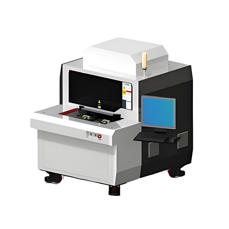
Can Locsen's equipment handle perovskite solar cells of varying sizes? What is the maximum supported dimension?
Locsen's laser equipment features exceptional size compatibility, capable of processing perovskite solar cells ranging from 10cm×10cm to 2.4m×1.2m.
For oversized cell processing (e.g., 12m×2.4m rigid substrates), we offer customized gantry-type laser systems with multi-laser-head synchronization to ensure both precision and throughput.
• Proven Performance: Successfully processed 1.2m×0.6m cells with industry-leading scribing accuracy (±15μm) and uniformity (>98%)
• Modular Design: Swappable optical modules adapt to varying thicknesses (0.1-6mm)
• Smart Calibration: AI-assisted real-time beam alignment compensates for substrate warpage
Does Locsen provide tailored laser solutions for all key production stages of perovskite solar cells?
Yes, Locsen provides comprehensive laser processing solutions covering the entire perovskite solar cell production chain:
P0 Laser Marking: For cell identification post-film deposition
P1/P2/P3 Laser Scribing: Precision patterning of
• Transparent conductive layers (P1)
• Perovskite active layers (P2)
• Back electrodes (P3)
P4 Edge Isolation: Micron-level edge trimming to prevent short-circuiting
Tandem Cell Modules: Dedicated laser etching systems for multi-material layer processing
Our integrated equipment ecosystem ensures all laser processing requirements are met with:
• ≤20μm alignment accuracy across layers
• Thermal Affect Zone controlled under 5μm
• Modular platforms supporting R&D to GW-scale production
What composition tolerance ranges do Locsen's tools support for variant perovskite formulations?
Locsen's laser systems demonstrate exceptional adaptability to diverse perovskite compositions.
• Preloaded Parameters: Optimized settings for mainstream formulations (e.g., FAPbI₃, CsPbI₃) in the laser recipe library enable instant operator access
• R&D Support: For novel compositions (e.g., Sn-based perovskites), our team delivers:
Custom wavelength/fluence calibration within 72 hours
Performance validation ensuring <1% PCE degradation post-processing
• Smart Compensation: On-board spectroscopy modules monitor reflectivity in real-time, automatically adjusting:
Pulse duration (20-500ns)
Beam profile (Top-hat/Gaussian)
Energy density (0.5-3J/cm²)
Technical Highlights:
▸ Tolerance for ±15% stoichiometric variation in Pb:Sn ratios
▸ Support for 2D/3D hybrid phase patterning
▸ Non-contact processing avoids cross-contamination


 Cell Laser Scribing Machine")


 Co., Ltd.")