


40px
80px
80px
80px
Lecheng Intelligent Technology Suzhou
Phone
+86-17751173582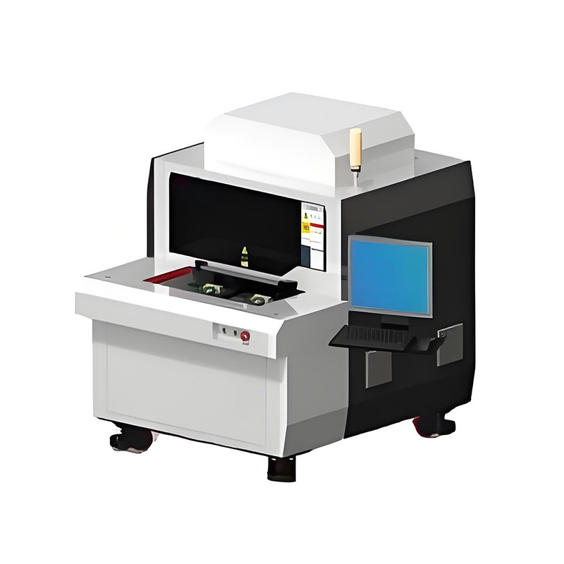
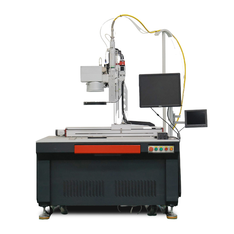
Dual-Station Solder Paste Laser Welder is designed for industrial laser processing projects that require stable beam control, process repeatability, and reliable integration with production requirements. For └ Laser Welding Equipment selection, buyers should compare material type, processing accuracy, automation level, throughput, maintenance access, and after-sales support before confirming the final equipment configuration.
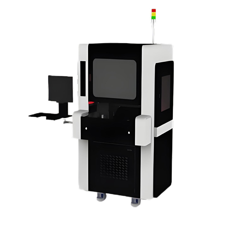
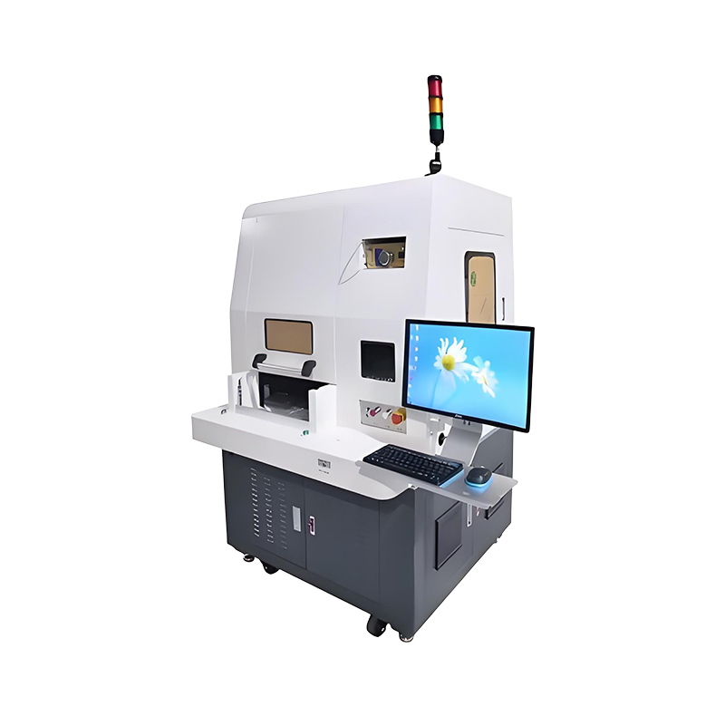
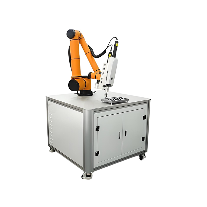
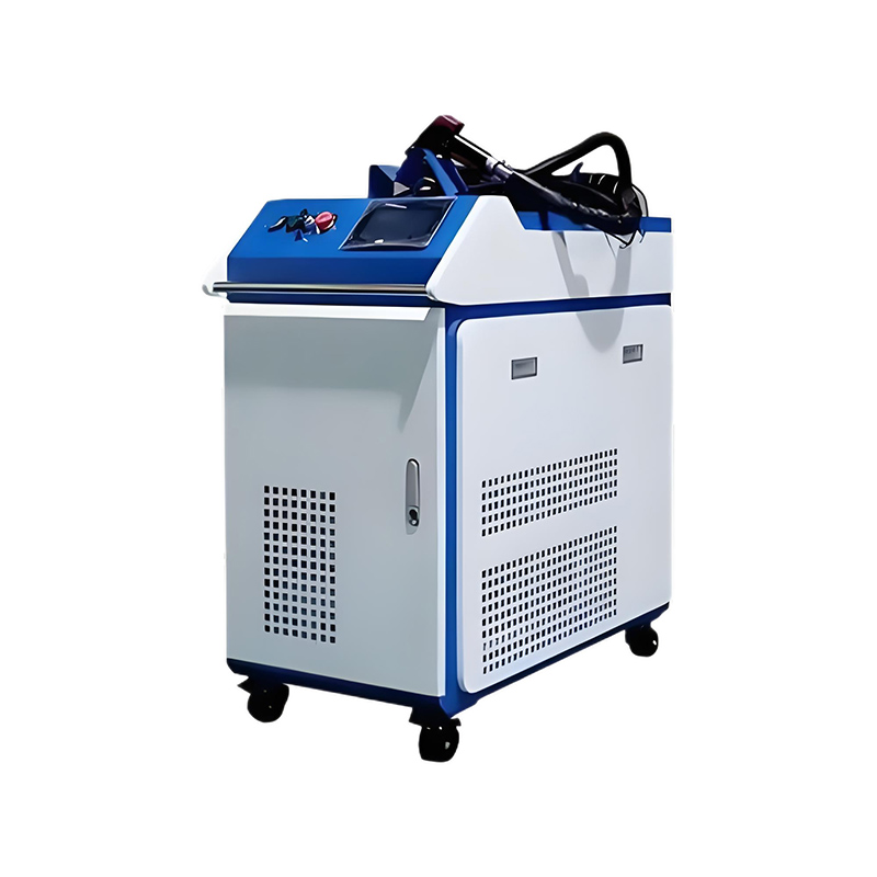
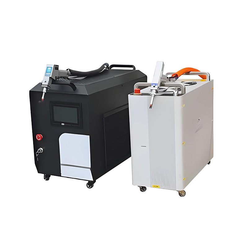
Related laser solutions include Portable Laser Welding Machine Handheld Laser Welder, Air-Cooled Handheld Laser Welding Machine, Robotic Laser Welding Cell. These internal references help users compare similar systems and move naturally between cleaning, cutting, scribing, marking, welding, and photovoltaic laser equipment pages.
The Dual-Station Solder Paste Laser Welding Equipment integrates a high-precision closed-loop temperature feedback system for real-time thermal regulation. Its automated tri-functional process enables seamless auto-positioning, precision solder paste dispensing, and laser welding execution within a single workflow. The core mechanical innovation lies in its synchronized dual-station architecture, allowing parallel processing operations while maintaining micron-level positioning accuracy (±5μm). Modular tooling stations support rapid fixture changeovers for diverse product geometries, and industrial-grade galvanometer scanning ensures consistent beam focal control across both stations.

Zero Thermal Damage Guarantee
Closed-loop temperature control actively prevents component burnout (ΔT≤±0.5°C), achieving >99.8% defect-free welds even on heat-sensitive substrates.
45% Operational Efficiency Boost
Concurrent dual-station processing eliminates idle time, completing 27-second cycle operations with automated material handling.
60% Cost Reduction
Dual-station workflow slashes labor requirements by 2 operators per shift and cuts energy consumption by 35% versus single-station systems.
Process Stability
Patented anti-dispersion laser optics maintain consistent spot size (<20μm variation) across 100,000+ weld cycles.

3C Electronics Manufacturing
Micro-welding of smartphone battery connectors (<0.3mm joints)
Camera module FPC bonding with ≤10μm positional accuracy
Automotive Micro-Components
Sensor housing hermetic sealing
ECU chip pin reflow without board deformation
Medical Device Assembly
Endoscope instrument welding (biocompatible Sn-Ag-Cu solder)
Implantable device encapsulation at ISO Class 5 cleanroom standards
Precision Industrial Components
Aerospace relay contacts (Cratering prevention)
Miniature relay welding under 5x magnification QA
40px
80px
80px
80px
Lecheng Intelligent Technology Suzhou
Phone
+86-17751173582