


40px
80px
80px
80px
Lecheng Intelligent Technology Suzhou
Phone
+86-17751173582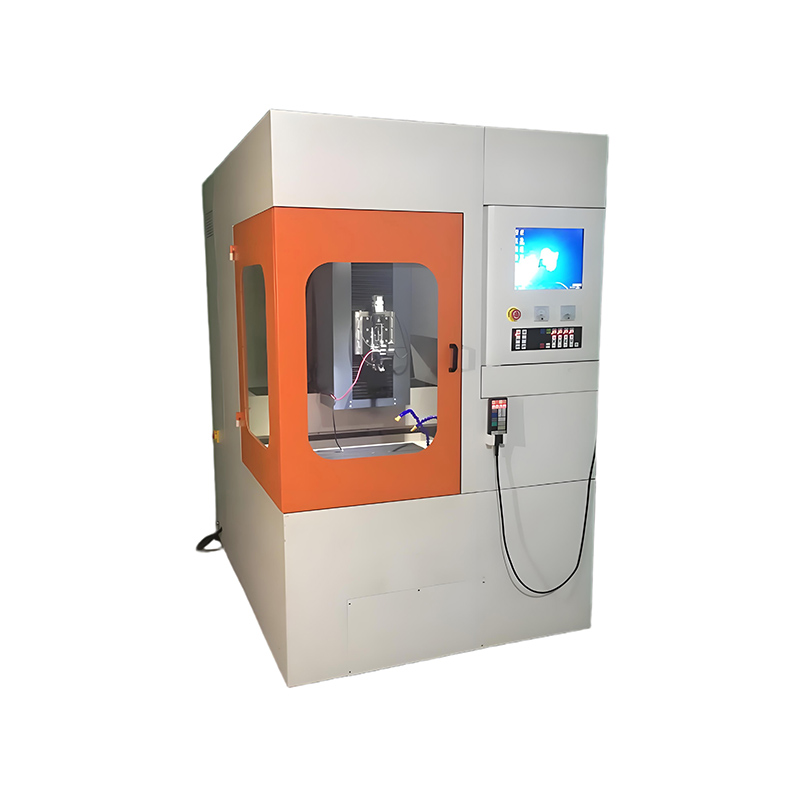
HDI Microvia Drilling Equipment is designed for industrial laser processing projects that require stable beam control, process repeatability, and reliable integration with production requirements. For ├ Laser Integrated Processing selection, buyers should compare material type, processing accuracy, automation level, throughput, maintenance access, and after-sales support before confirming the final equipment configuration.
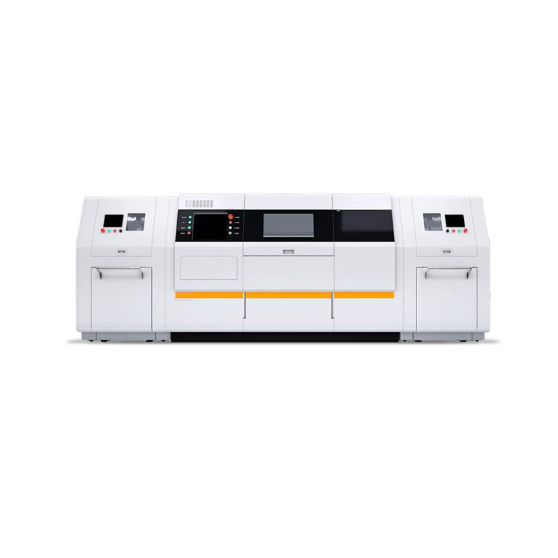
Related laser solutions include Consumer Electronics Laser Drilling Equipment, PCB Drilling Equipment, Laser Optics and Accessories. These internal references help users compare similar systems and move naturally between cleaning, cutting, scribing, marking, welding, and photovoltaic laser equipment pages.
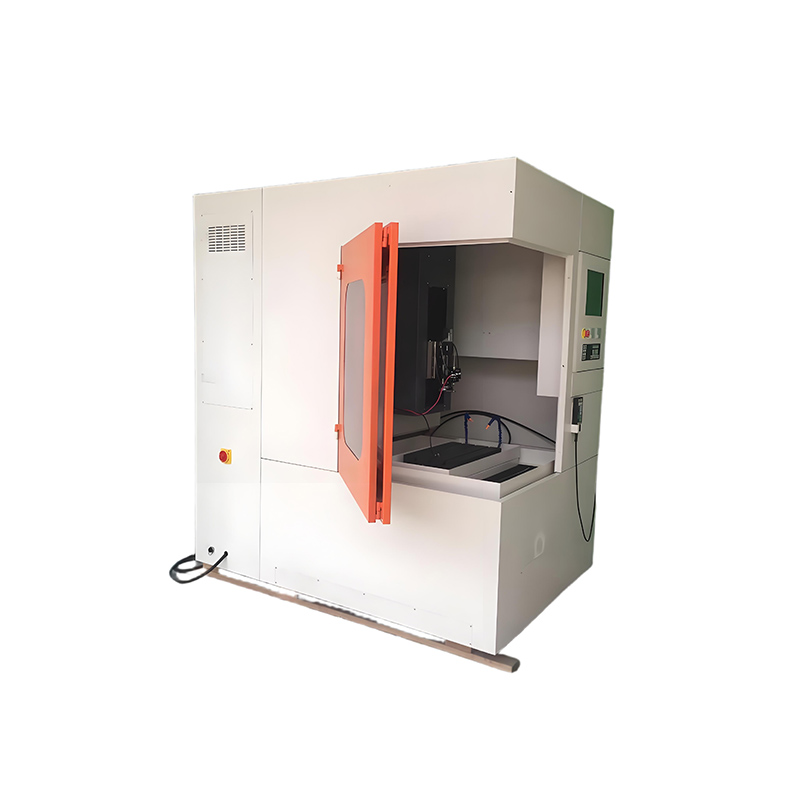
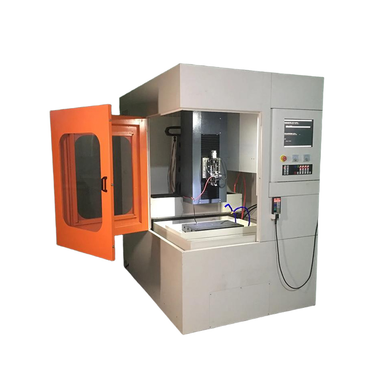
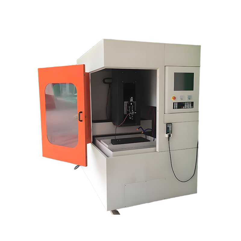
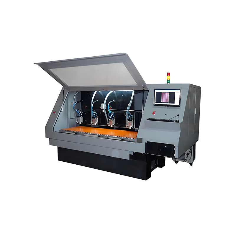
The HDI Microvia Drilling Equipment is a high-precision laser processing system specifically designed for high-density interconnect (HDI) boards. Featuring advanced UV laser technology combined with precision positioning stages and intelligent control systems, it achieves microvia drilling as small as 25μm, making it ideal for 5G communication devices and premium smartphone motherboards.


Laser System:
355nm UV nanosecond/picosecond laser
Beam quality M²<1.3, adjustable spot size (10-50μm)
±2% pulse energy stability
Motion System:
High-precision linear motor stages
±5μm positioning accuracy, ±2μm repeatability
Maximum acceleration of 2m/s²
Vision System:
10MP high-resolution CCD camera
±2μm auto-focus accuracy
PCB expansion compensation
Control System:
Industrial-grade motion controller
Direct Gerber file import
Automatic path optimization
Specification | Parameter | Benefit |
|---|---|---|
Minimum Via Size | 25μm | Meets ultra-HDI requirements |
Position Accuracy | ±5μm | Ensures layer-to-layer alignment |
Processing Speed | 500 holes/sec | High production throughput |
Via Wall Quality | Ra<1μm | Reduces plating difficulty |
Equipment Uptime | >95% | Guarantees production stability |

Key Advantages:
Non-contact processing eliminates mechanical stress
Automatic material expansion compensation
Intelligent energy control for consistent via shape
Modular design for easy maintenance
Communication Equipment:
5G base station PCBs
Millimeter-wave antenna boards
Consumer Electronics:
Smartphone motherboards
Wearable device flex boards
Automotive Electronics:
Vehicle radar PCBs
New energy vehicle control modules
Aerospace/Military:
High-reliability military PCBs
Satellite communication boards
40px
80px
80px
80px
Lecheng Intelligent Technology Suzhou
Phone
+86-17751173582