


40px
80px
80px
80px
Lecheng Intelligent Technology Suzhou
Phone
+86-17751173582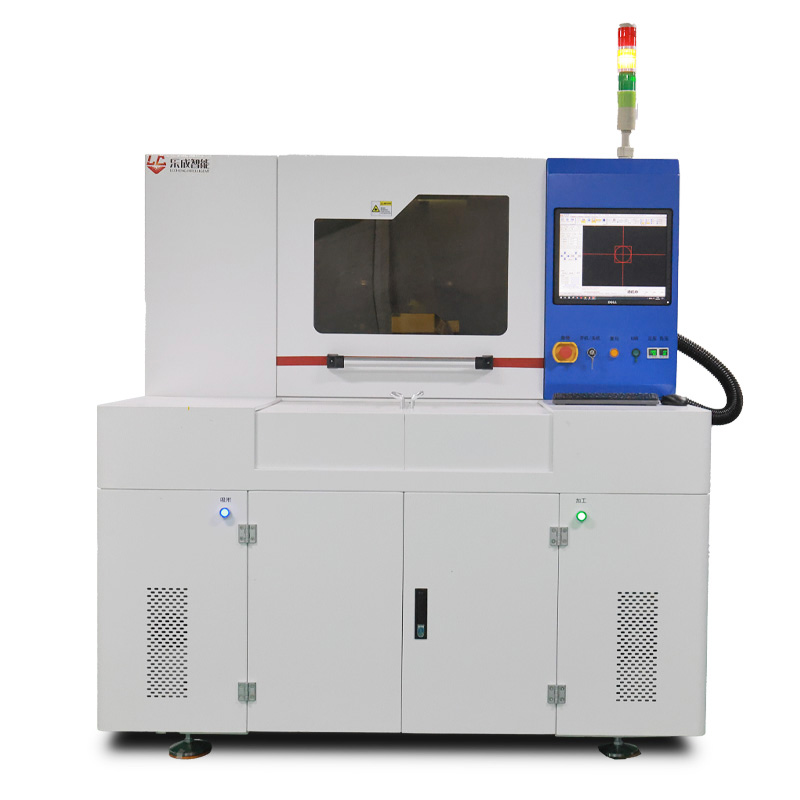


Integrated Processing Equipment for Thin-Film Solar Cells is designed for industrial laser processing projects that require stable beam control, process repeatability, and reliable integration with production requirements. For ├ Laser Scribing Equipment selection, buyers should compare material type, processing accuracy, automation level, throughput, maintenance access, and after-sales support before confirming the final equipment configuration.
Related laser solutions include Roll to Roll Laser Scribing Edge Cleaning System, Photovoltaic (PV) Cell Laser Scribing Machine, Fully Automatic Thin Film Photovoltaic Laser Scribing Equipment. These internal references help users compare similar systems and move naturally between cleaning, cutting, scribing, marking, welding, and photovoltaic laser equipment pages.
The FCC-05 Series Laser Integrated Processing System is a cutting-edge dual-optical-path platform designed for R&D and production of thin-film solar cells. Its core components include:
Dual-Laser Configuration: Integrates a fiber nanosecond laser and ultrafast pulsed laser (wavelength options: 1064nm/532nm/355nm) for versatile processing.
Precision Mechanics: Offers a 500mm×500mm(max) processing area with <30μm feature resolution and ±5μm positioning accuracy, enabled by multi-mode positioning technology.
Modular Integration: Combines an automated control system, high-speed optical processing unit, and machine vision alignment system in a compact, stable frame.
Proprietary Software: Features self-developed control software with intuitive HMI for customizable process workflows.
Key innovations include the simultaneous P1/P2/P3 laser scribing and P4 edge isolation capability, achieved through synchronized dual-beam processing—a critical advantage for thin-film solar cell manufacturing.

Unmatched Stability:
Advanced motion control hardware (e.g., linear encoders, vibration-damped stages) ensures 24/7 operational reliability even in high-throughput environments.
Seamless subsystem integration minimizes downtime.
Process Flexibility:
Wavelength-switching capability (IR/visible/UV) adapts to diverse thin-film materials (CIGS, CdTe, perovskite).
Programmable parameters (pulse width, energy, overlap) via proprietary software enable R&D-grade tunability.
Precision Engineering:
Multi-sensor feedback (CCD alignment, laser interferometry) guarantees sub-5μm repeatability for critical scribing tasks.
Dynamic focus control maintains consistency across uneven substrates.
Future-Ready Design:
Supports AI-driven process optimization and IoT connectivity for Industry 4.0 integration.
Primarily deployed for:
Thin-Film Solar Cell R&D: Accelerates process development for small-format solar modules, including:
P1-P4 patterning (transparent conductive oxide, absorber, back-contact layers).
Edge isolation with minimized thermal damage (<50μm heat-affected zone).
Pilot Production: Serves as a bridge between lab-scale and mass production, offering:
Process validation for new materials (e.g., perovskite tandem cells).
High-yield prototyping (up to 98% scribing accuracy).
Quality Control:
In-line defect detection via integrated imaging systems.
Non-contact processing eliminates mechanical stress on fragile substrates.
Industry Impact: This system addresses key challenges in thin-film solar manufacturing—throughput bottlenecks, layer alignment errors, and edge recombination losses—while reducing production costs by up to 20% compared to conventional multi-step systems.
40px
80px
80px
80px
Lecheng Intelligent Technology Suzhou
Phone
+86-17751173582