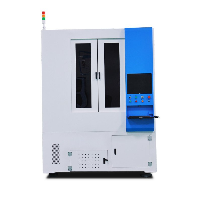
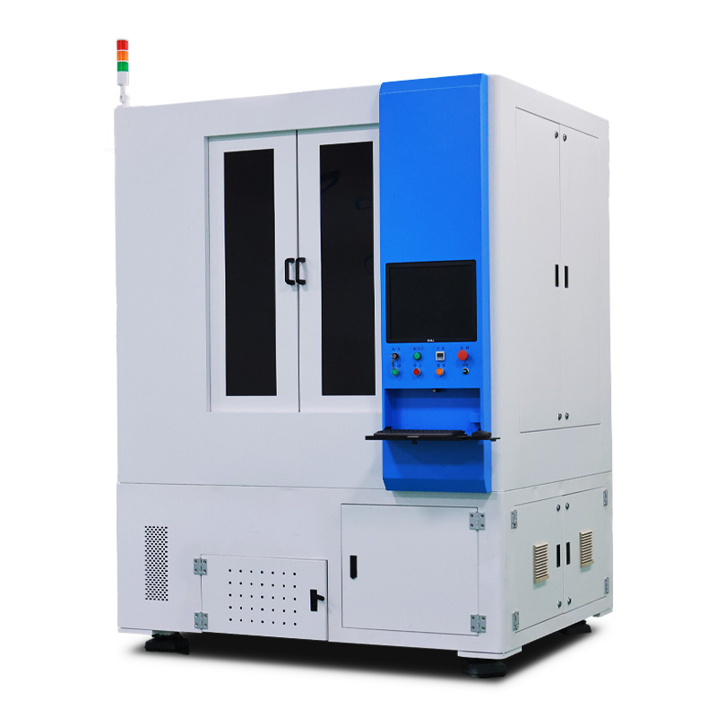
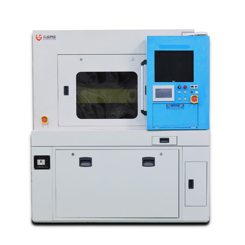
Products

Featured products

Contact us

  • Laser Etching Equipment​
  • Laser Etching Equipment​
  • Laser Etching Equipment​
  • video

Laser Etching Equipment​

Ultrafine 5μm Laser Etching—Sub-micron precision for semiconductors & FPCs. 2000mm/s High-Speed Processing—4x faster vs chemical etching, zero waste. 200+ Material Compatibility—From glass to titanium alloys, non-contact. Intelligent HMI Control—Auto-focus & CAD integration, ISO certified.
  • Le Cheng
  • Shanghai
  • Three months
  • Fifty sets within the year

Structural Features

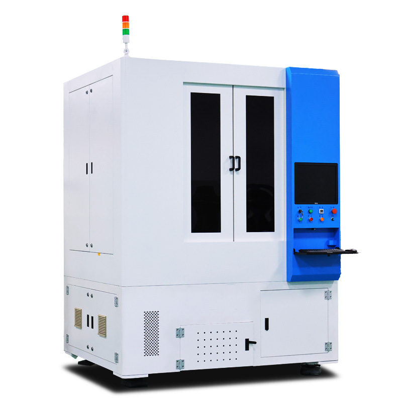
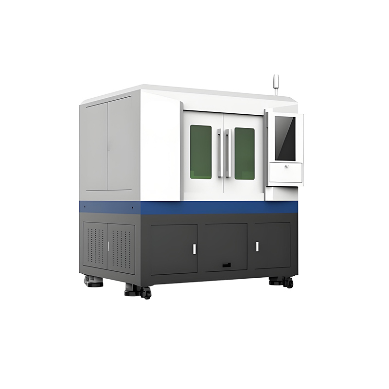
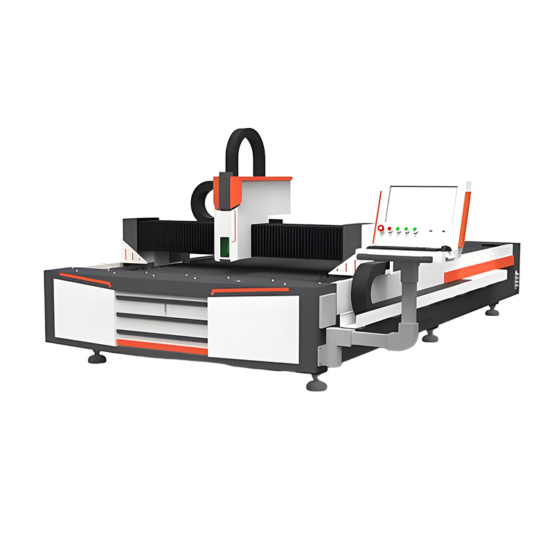
Our laser etching system integrates cutting-edge engineering for unparalleled performance:

  1. Ultra-Stable Laser Source: Fiber/UV/Picosecond lasers with adjustable pulse duration (ns/ps/fs), wavelength options (355nm, 532nm, 1064nm), and peak power up to 50W.

  2. High-Precision Motion System: Air-bearing granite stage with ±1μm positioning accuracy, coupled with galvanometer scanning (7mm²–300mm² FOV) for dynamic patterning.

  3. Intelligent Control Suite:

    • Real-time Z-axis autofocus (resolution: 0.1μm)

    • CCD vision alignment for ±5μm overlay accuracy

    • HMI with proprietary software supporting DXF, Gerber, BMP formats

  4. Multi-Layer Environmental Control:

    • Class 1000 cleanroom-compatible enclosure

    • Active temperature-humidity regulation (±0.5°C)

    • Integrated fume extraction with HEPA filtration

  5. Modular Upgrade Path: Optional 3-axis rotary stage, in-situ profilometry, or multi-laser hybrid configuration.

  6. Laser Etching Equipment​


Technical Advantages

Revolutionize your manufacturing with core technological edges:

  • Sub-Micron Precision: Achieve 5–20μm feature sizes (Ra < 0.2μm) through diffraction-limited beam shaping.

  • Zero-Contact Processing: Eliminate tool wear and mechanical stress for brittle materials (e.g., SiC, glass).

  • Adaptive Energy Control: Pulse-by-pulse power modulation (1–100% in 0.1% steps) enables selective ablation of multilayers (e.g., ITO/Ag/PET).

  • Speed & Efficiency: 2000 mm/s scan speed with 50g acceleration; 4x faster than chemical etching.

  • Eco-Conscious Operation: 30% lower energy consumption vs. competitors; no toxic etchants or wastewater.

precision laser etching

Typical Applications

Empowering innovation across industries:


SectorUse CasesKey Benefits
SemiconductorsWafer dicing, IC trimming, package marking<10μm kerf width, zero micro-cracks
FPD/LEDFPC patterning, OLED encapsulation removal, touch sensor etchingSelective ablation, 99.9% yield rate
SolarPERC cell drilling (10–20μm holes), thin-film scribing500 holes/sec, ±2μm positional accuracy
Medical DevicesStent texturing, implant micro-grooving, lab-on-chip channel fabricationBiocompatible surface modification
Advanced R&D2D material processing, metasurface creation, quantum device prototypingNanosecond thermal im


Specifications are indicative only - All equipment is fully customizable to your needs!


Get Quote

  • How long does it take from equipment ordering to official production when cooperating with Locsen?

    The overall timeline varies depending on equipment specifications and production line scale. For standalone equipment, standard models require a 45-day manufacturing cycle, with total duration (including shipping and installation) of approximately 60 days. Customized equipment requires an additional 30 days based on technical requirements. For complete line solutions: • 100MW-level production lines require ~4 months for planning, equipment manufacturing, installation, and commissioning • GW-level production lines require ~8 months We provide detailed project schedules with dedicated managers ensuring seamless coordination. Example: A client's 1GW perovskite production line was completed 15 days ahead of schedule through parallel equipment manufacturing and facility construction.
  • Does Locsen offer suitable equipment and partnership solutions for startup perovskite companies

    Locsen offers a "Phased Partnership Program" specifically designed for perovskite startups. For the initial R&D phase, we provide compact pilot-scale equipment (e.g., 10MW laser scribing systems) bundled with essential process packages to facilitate technology validation and product iteration. During scale-up phases, startups qualify for upgrade benefits: • Core modules from pilot equipment can be traded in with value deduction toward production-line machinery • Optional technical collaboration including process development support and experimental data sharing This program has successfully enabled multiple startups to transition smoothly from lab to pilot production while mitigating early-stage investment risks.
  • Can Locsen's equipment handle perovskite solar cells of varying sizes? What is the maximum supported dimension?

    Locsen's laser equipment features exceptional size compatibility, capable of processing perovskite solar cells ranging from 10cm×10cm to 2.4m×1.2m. For oversized cell processing (e.g., 12m×2.4m rigid substrates), we offer customized gantry-type laser systems with multi-laser-head synchronization to ensure both precision and throughput. • Proven Performance: Successfully processed 1.2m×0.6m cells with industry-leading scribing accuracy (±15μm) and uniformity (>98%) • Modular Design: Swappable optical modules adapt to varying thicknesses (0.1-6mm) • Smart Calibration: AI-assisted real-time beam alignment compensates for substrate warpage
  • Does Locsen provide tailored laser solutions for all key production stages of perovskite solar cells?

    Yes, Locsen provides comprehensive laser processing solutions covering the entire perovskite solar cell production chain: P0 Laser Marking: For cell identification post-film deposition P1/P2/P3 Laser Scribing: Precision patterning of • Transparent conductive layers (P1) • Perovskite active layers (P2) • Back electrodes (P3) P4 Edge Isolation: Micron-level edge trimming to prevent short-circuiting Tandem Cell Modules: Dedicated laser etching systems for multi-material layer processing Our integrated equipment ecosystem ensures all laser processing requirements are met with: • ≤20μm alignment accuracy across layers • Thermal Affect Zone controlled under 5μm • Modular platforms supporting R&D to GW-scale production
  • What composition tolerance ranges do Locsen's tools support for variant perovskite formulations?

    Locsen's laser systems demonstrate exceptional adaptability to diverse perovskite compositions. • Preloaded Parameters: Optimized settings for mainstream formulations (e.g., FAPbI₃, CsPbI₃) in the laser recipe library enable instant operator access • R&D Support: For novel compositions (e.g., Sn-based perovskites), our team delivers: Custom wavelength/fluence calibration within 72 hours Performance validation ensuring <1% PCE degradation post-processing • Smart Compensation: On-board spectroscopy modules monitor reflectivity in real-time, automatically adjusting: Pulse duration (20-500ns) Beam profile (Top-hat/Gaussian) Energy density (0.5-3J/cm²) Technical Highlights: ▸ Tolerance for ±15% stoichiometric variation in Pb:Sn ratios ▸ Support for 2D/3D hybrid phase patterning ▸ Non-contact processing avoids cross-contamination

Related Products

40px

80px

80px

80px

Get Quote