Products

Featured products

Contact us

  • Fully Automatic Thin Film Photovoltaic Laser Scribing Equipment
  • Fully Automatic Thin Film Photovoltaic Laser Scribing Equipment
  • Fully Automatic Thin Film Photovoltaic Laser Scribing Equipment
  • Fully Automatic Thin Film Photovoltaic Laser Scribing Equipment
  • video

Fully Automatic Thin Film Photovoltaic Laser Scribing Equipment

Fully automatic thin film photovoltaic laser scribing equipment supports precise P1 P2 P3 patterning for PV module production. Stable laser processing helps improve cell consistency edge quality and production efficiency. Suitable for perovskite thin film solar and photovoltaic manufacturing lines.

    Fully Automatic Thin Film Photovoltaic Laser Scribing Equipment application and selection guide

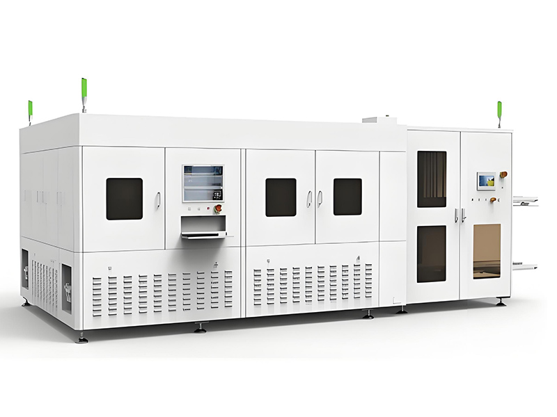
    Fully Automatic Thin Film Photovoltaic Laser Scribing Equipment is designed for industrial laser processing projects that require stable beam control, process repeatability, and reliable integration with production requirements. For ├ Perovskite Laser Production Line selection, buyers should compare material type, processing accuracy, automation level, throughput, maintenance access, and after-sales support before confirming the final equipment configuration.

    Related laser solutions include Multi Channel Photovoltaic IV MPPT Test System for Low Light Conditions, Outdoor Multi-Channel PV Module Aging Test System, Multi-Channel PV Module Steady-State Test System. These internal references help users compare similar systems and move naturally between cleaning, cutting, scribing, marking, welding, and photovoltaic laser equipment pages.

    Fully Automatic Thin-Film Battery Laser Scribing Equipment

    Precision Engineering for Next-Generation Battery Manufacturing


    Structural Features

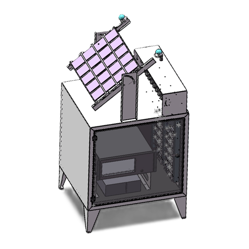
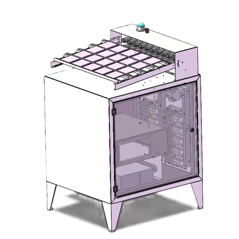
    Our laser scribing system features an innovative three-station configuration (loading/scribing/unloading) designed for maximum throughput and reliability. The equipment boasts:

    • Large-format processing capacity: Accommodates panels up to 2.4×1.2 meters

    • Advanced optical system: 24-beam laser splitting with adjustable spacing (50-500μm)

    • Controlled environment: Fully enclosed Class 1000 (ISO 6) cleanroom-compatible structure

    • Modular architecture: Quick-change laser source and optical module interfaces

    • Precision motion system: Linear motors with 0.1μm resolution encoders

    The rigid aluminum alloy frame with vibration damping ensures stable operation at speeds up to 2m/s while maintaining ±5μm positioning accuracy.

    Thin Film Photovoltaic Laser ScribingPerovskite Laser Scribing Equipment


    Product Advantages

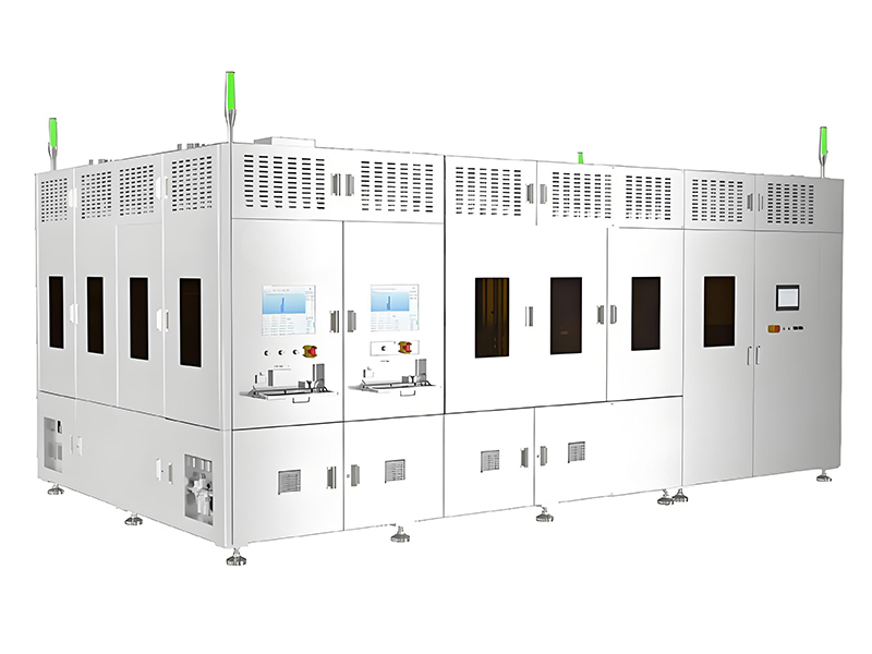
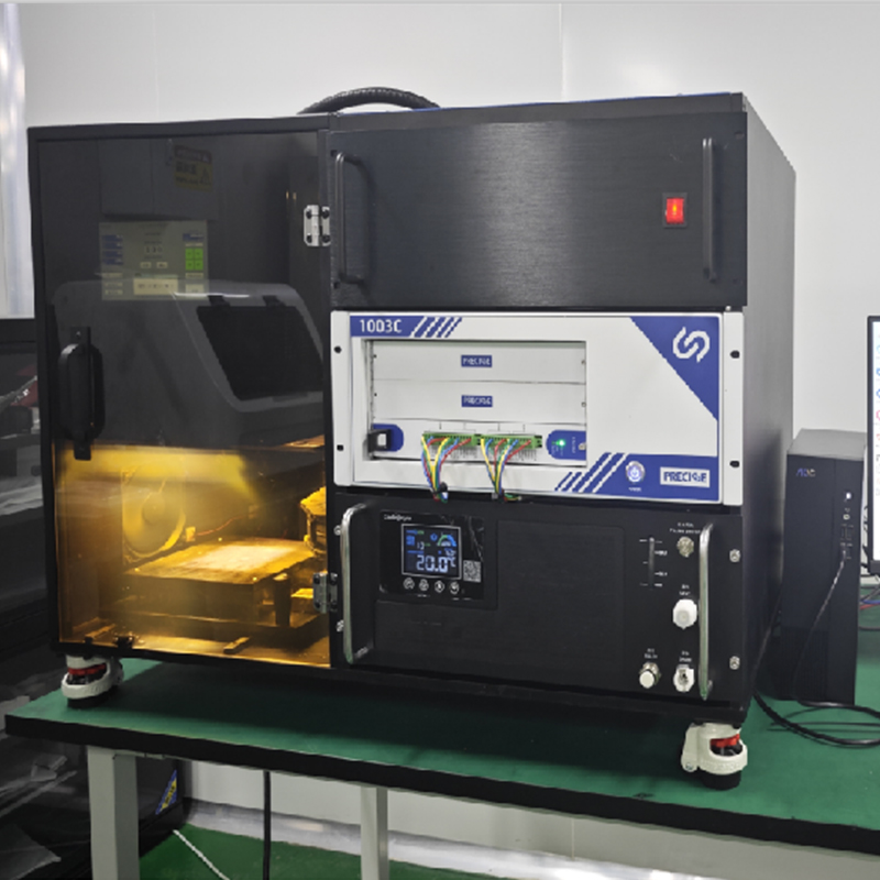
    Engineered for superior performance and cost efficiency:
    Multi-process compatibility: Supports IR (1064nm), green (532nm), and UV (355nm) lasers for different materials
    Intelligent control system: Proprietary software with AI-based process optimization
    Enhanced uptime: <15min module changeover time and predictive maintenance alerts
    Ultra-precise alignment: Combines vision, laser, and mechanical positioning (±3μm repeatability)
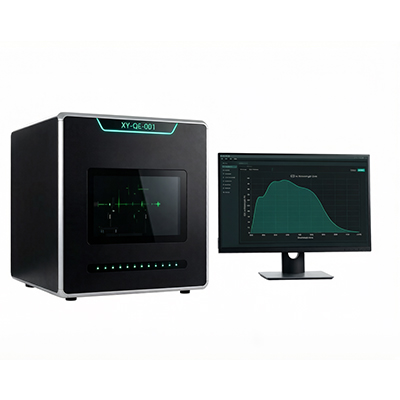
    Smart monitoring: 4K imaging with defect detection algorithms and cloud data storage

    The unified platform reduces total cost of ownership by 30% compared to conventional systems through shared infrastructure and reduced maintenance requirements.

    PV Laser Scribing Machine

    Thin Film Photovoltaic Laser Scribing


    Product Applications


    Ideal for advanced energy storage and electronic device manufacturing:


    Energy Storage Solutions
    • P1/P2/P3 patterning for lithium polymer batteries

    • Insulation trench creation in solid-state batteries
    • Tab welding preparation for EV battery packs

    Flexible Electronics
    • Flexible circuit isolation for wearables
    • RFID antenna patterning
    • Medical sensor fabrication

    Photovoltaics
    • CIGS solar cell segmentation
    • Perovskite module interconnection
    • Transparent conductive oxide scribing

    Optional configurations for specific industry requirements.


    Perovskite Laser Scribing Equipment


    Get Quote

    • How long does it take from equipment ordering to official production when cooperating with Locsen?

      The overall timeline varies depending on equipment specifications and production line scale. For standalone equipment, standard models require a 45-day manufacturing cycle, with total duration (including shipping and installation) of approximately 60 days. Customized equipment requires an additional 30 days based on technical requirements. For complete line solutions: • 100MW-level production lines require ~4 months for planning, equipment manufacturing, installation, and commissioning • GW-level production lines require ~8 months We provide detailed project schedules with dedicated managers ensuring seamless coordination. Example: A client's 1GW perovskite production line was completed 15 days ahead of schedule through parallel equipment manufacturing and facility construction.
    • Does Locsen offer suitable equipment and partnership solutions for startup perovskite companies

      Locsen offers a "Phased Partnership Program" specifically designed for perovskite startups. For the initial R&D phase, we provide compact pilot-scale equipment (e.g., 10MW laser scribing systems) bundled with essential process packages to facilitate technology validation and product iteration. During scale-up phases, startups qualify for upgrade benefits: • Core modules from pilot equipment can be traded in with value deduction toward production-line machinery • Optional technical collaboration including process development support and experimental data sharing This program has successfully enabled multiple startups to transition smoothly from lab to pilot production while mitigating early-stage investment risks.
    • Can Locsen's equipment handle perovskite solar cells of varying sizes? What is the maximum supported dimension?

      Locsen's laser equipment features exceptional size compatibility, capable of processing perovskite solar cells ranging from 10cm×10cm to 2.4m×1.2m. For oversized cell processing (e.g., 12m×2.4m rigid substrates), we offer customized gantry-type laser systems with multi-laser-head synchronization to ensure both precision and throughput. • Proven Performance: Successfully processed 1.2m×0.6m cells with industry-leading scribing accuracy (±15μm) and uniformity (>98%) • Modular Design: Swappable optical modules adapt to varying thicknesses (0.1-6mm) • Smart Calibration: AI-assisted real-time beam alignment compensates for substrate warpage
    • Does Locsen provide tailored laser solutions for all key production stages of perovskite solar cells?

      Yes, Locsen provides comprehensive laser processing solutions covering the entire perovskite solar cell production chain: P0 Laser Marking: For cell identification post-film deposition P1/P2/P3 Laser Scribing: Precision patterning of • Transparent conductive layers (P1) • Perovskite active layers (P2) • Back electrodes (P3) P4 Edge Isolation: Micron-level edge trimming to prevent short-circuiting Tandem Cell Modules: Dedicated laser etching systems for multi-material layer processing Our integrated equipment ecosystem ensures all laser processing requirements are met with: • ≤20μm alignment accuracy across layers • Thermal Affect Zone controlled under 5μm • Modular platforms supporting R&D to GW-scale production
    • What composition tolerance ranges do Locsen's tools support for variant perovskite formulations?

      Locsen's laser systems demonstrate exceptional adaptability to diverse perovskite compositions. • Preloaded Parameters: Optimized settings for mainstream formulations (e.g., FAPbI₃, CsPbI₃) in the laser recipe library enable instant operator access • R&D Support: For novel compositions (e.g., Sn-based perovskites), our team delivers: Custom wavelength/fluence calibration within 72 hours Performance validation ensuring <1% PCE degradation post-processing • Smart Compensation: On-board spectroscopy modules monitor reflectivity in real-time, automatically adjusting: Pulse duration (20-500ns) Beam profile (Top-hat/Gaussian) Energy density (0.5-3J/cm²) Technical Highlights: ▸ Tolerance for ±15% stoichiometric variation in Pb:Sn ratios ▸ Support for 2D/3D hybrid phase patterning ▸ Non-contact processing avoids cross-contamination

    Related Products

    40px

    80px

    80px

    80px

    Get Quote