


40px
80px
80px
80px
Lecheng Intelligent Technology Suzhou
Phone
+86-17751173582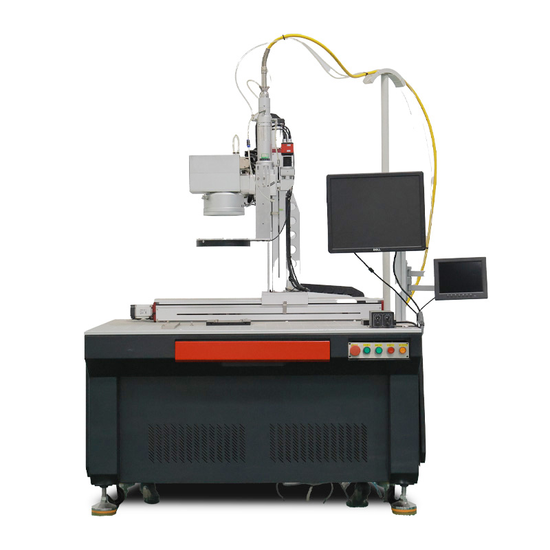

Laser Welding Equipment is designed for industrial laser processing projects that require stable beam control, process repeatability, and reliable integration with production requirements. For └ Laser Welding Equipment selection, buyers should compare material type, processing accuracy, automation level, throughput, maintenance access, and after-sales support before confirming the final equipment configuration.
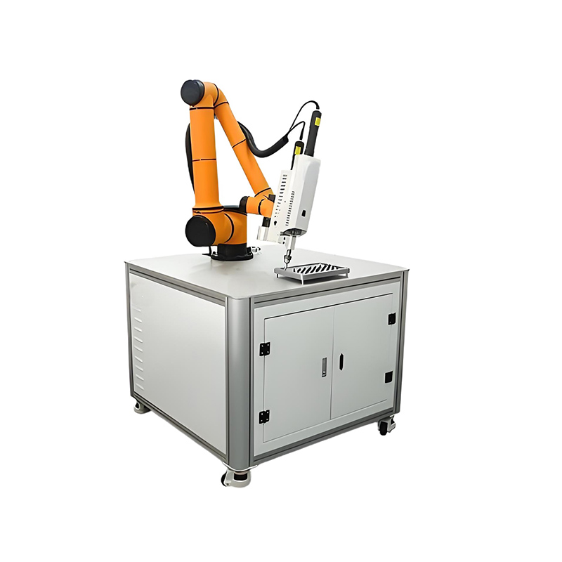
Related laser solutions include Air-Cooled Handheld Laser Welding Machine, Portable Laser Welding Machine Handheld Laser Welder, Robotic Laser Welding Cell. These internal references help users compare similar systems and move naturally between cleaning, cutting, scribing, marking, welding, and photovoltaic laser equipment pages.
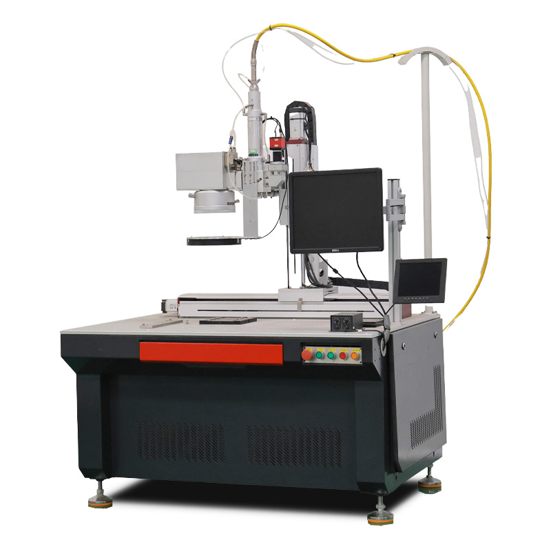
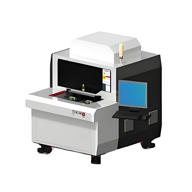
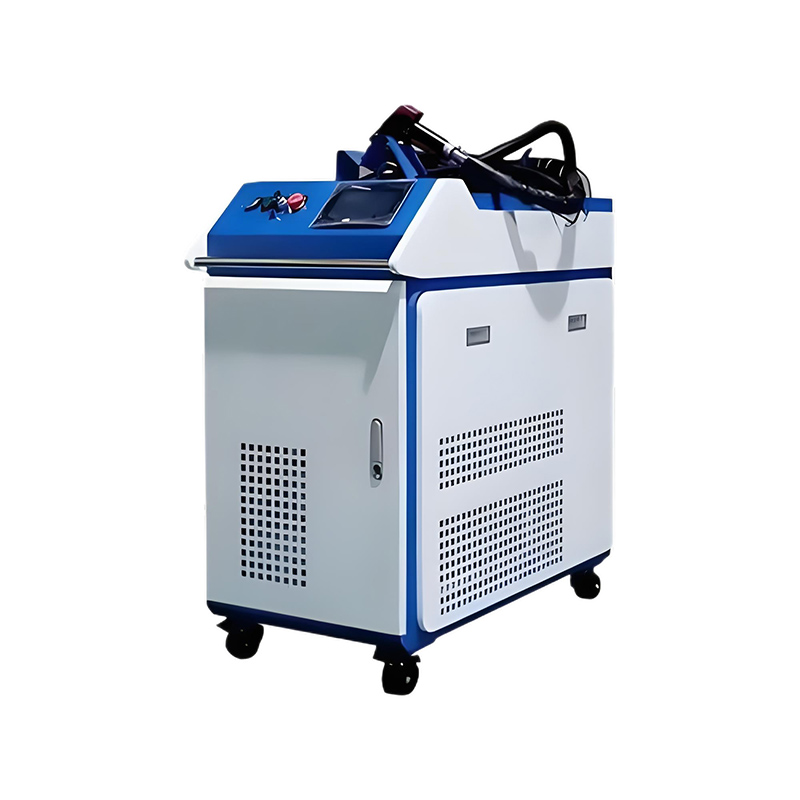
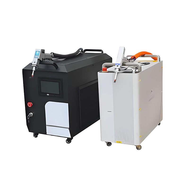
Laser welding equipment is a high-end manufacturing system that utilizes high-energy-density laser beams to achieve precision material joining. By focusing laser energy through advanced optical systems, the device enables rapid melting and fusion of metals or non-metals within milliseconds, offering core advantages such as high efficiency, precision, and non-contact processing. With exceptional process adaptability and automation capabilities, laser welding systems are widely adopted in high-value industries including automotive, consumer electronics, medical devices, and aerospace, making them a pivotal technology in modern smart manufacturing.

Modular Design: The system adopts a modular architecture, allowing flexible configuration of laser sources, welding heads, and motion control systems to meet diverse processing requirements.
High-Precision Motion System: Equipped with rigid robotic arms or linear motor stages, ensuring stability and repeatable micron-level positioning accuracy for delicate welding tasks.
Intelligent Control System: Integrated PLC and industrial PC enable automated programming and real-time monitoring, featuring seam tracking and adaptive power adjustment for consistent weld quality.
User-Friendly Interface: A high-resolution touchscreen with intuitive HMI supports one-touch parameter setup and process database access, reducing operator training time.
Compact Footprint: Space-saving design facilitates integration into workshops or automated production lines.
High Efficiency & Energy Saving: Fiber or semiconductor lasers achieve over 30% electro-optical efficiency, reducing energy consumption by 50% compared to conventional methods.
Non-Contact Processing: Eliminates mechanical stress on workpieces, ideal for thin sheets and sensitive components like electronics.
Broad Material Compatibility: Welds reflective metals (aluminum, copper) and dissimilar materials via adjustable pulsed/continuous waveforms.
Eco-Friendly Operation: Minimizes consumables (e.g., filler wires) and emissions, aligning with sustainable manufacturing standards.
Process Reliability: Built-in temperature feedback and optical path calibration ensure defect-free seams (e.g., no porosity) during prolonged operation.
Automotive: Battery tab welding, lightweight structural component joining.
Consumer Electronics: Smartphone frames, camera modules, and flexible PCB soldering.
Medical Devices: Hermetic sealing of surgical tools and implantable devices.
Aerospace: High-temperature alloy welding for turbine blades and fuel conduits.
Household Hardware: Mass production of kitchenware seals and sensor housings.
40px
80px
80px
80px
Lecheng Intelligent Technology Suzhou
Phone
+86-17751173582