


40px
80px
80px
80px
Lecheng Intelligent Technology Suzhou
Phone
+86-17751173582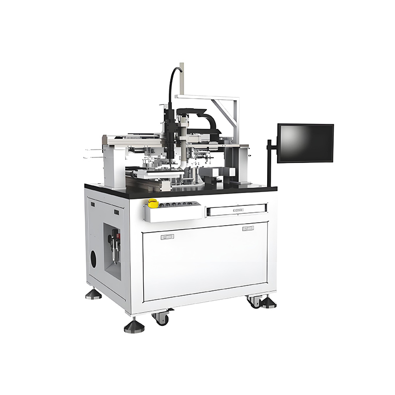
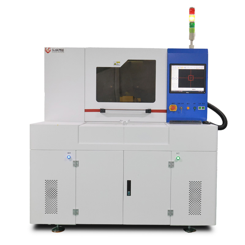
Photovoltaic (PV) Cell Laser Scribing Machine is designed for industrial laser processing projects that require stable beam control, process repeatability, and reliable integration with production requirements. For ├ Laser Scribing Equipment selection, buyers should compare material type, processing accuracy, automation level, throughput, maintenance access, and after-sales support before confirming the final equipment configuration.
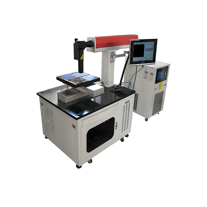
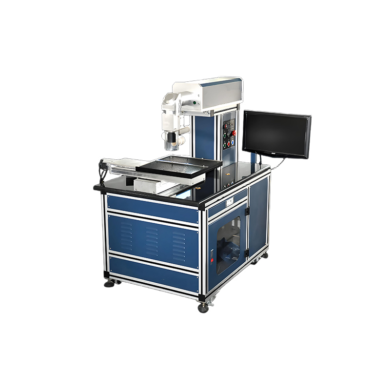
Related laser solutions include Roll to Roll Laser Scribing Edge Cleaning System, Integrated Processing Equipment for Thin-Film Solar Cells, Fully Automatic Thin Film Photovoltaic Laser Scribing Equipment. These internal references help users compare similar systems and move naturally between cleaning, cutting, scribing, marking, welding, and photovoltaic laser equipment pages.
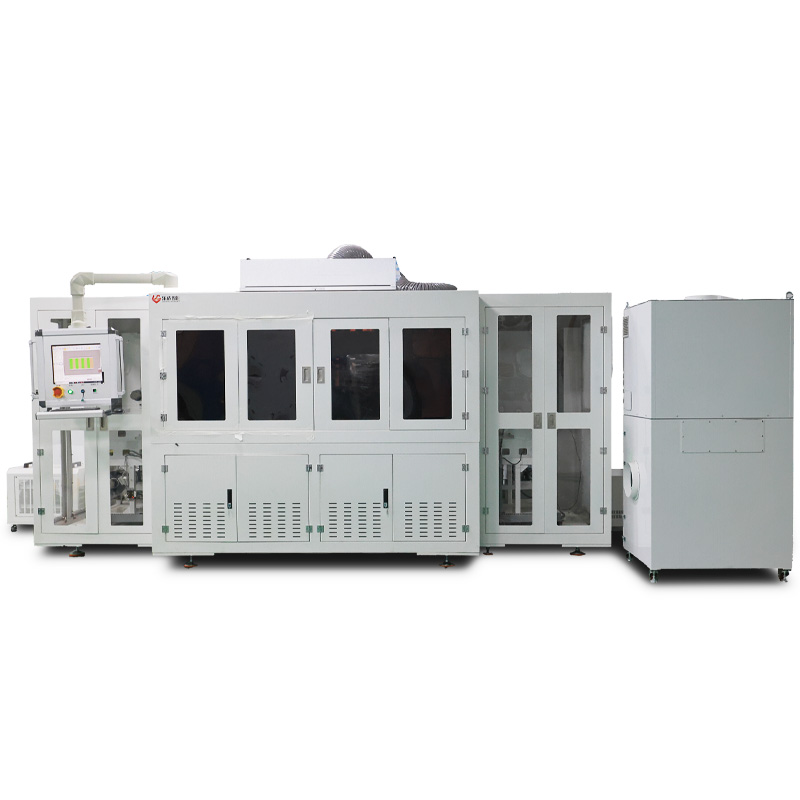
Overview
This laser scribing system utilizes multi-beam technology for damage-free segmentation of PERC/HJT/TOPCon solar cells. Compatible with M12 wafers (210mm) and featuring AI vision alignment, it maximizes yield while minimizing power loss for advanced module production.

Feature | Specification |
|---|---|
Laser System | Dual-head fiber (1064nm) |
Scribing Acc. | ±5μm (Micro-crack <20μm) |
Max Wafer Size | 230mm×230mm (G12 compatible) |
Throughput | 6000 wafers/hour |
Changeover Time | <5 minutes |
Performance Bars:
Precision: 8/10
Speed: 9/10
Compatibility: 7/10
Stability: 8/10

Ultra-High Yield:≥99.8% survival rate, saving $200k/year
Zero Power Loss:<0.2% degradation, +1.5W module gain
Dramatic Cost Cut:$0.01/wafer (60% lower vs diamond wire)
Smart Compensation:AI monitors HAZ, auto-adjusts energy
▶ PERC Cells:9BB/12BB half-cut scribing
▶ TOPCon Cells:Busbar-preserving segmentation
▶ HJT Cells:Low-temp precision patterning
▶ Perovskite:TCO layer structuring
40px
80px
80px
80px
Lecheng Intelligent Technology Suzhou
Phone
+86-17751173582