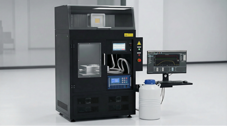
Cell Laser Scribing Machine")


 Co., Ltd.")
Technical Challenges and Innovations in Thin-Film Laser Etching Equipment
Laser etching technology has become indispensable in the precision processing of thin-film materials, particularly in industries such as display manufacturing, photovoltaics, and flexible electronics. Despite its advantages in non-contact processing, digital control, and high precision, several technical challenges persist in the development and application of thin-film laser etching equipment. This article explores these challenges and the innovative solutions driving the industry forward.

1. Thermal Management and Heat-Affected Zone (HAZ) Control
Challenge:
Laser etching generates significant heat, which can cause thermal damage to both the thin film and the substrate. This includes material deformation, microcracks, and changes in material properties. The heat-affected zone (HAZ) must be minimized to ensure edge quality and functional integrity.
Solutions:
Ultrafast Lasers: Femtosecond or picosecond lasers reduce HAZ by limiting thermal diffusion through ultra-short pulse durations (e.g., 300 fs).
Pulse Burst Mode: Replacing single high-energy pulses with multiple low-energy pulses (Burst Mode) distributes energy more evenly, reducing peak temperatures and HAZ.
Cooling Systems: Integrated liquid cooling or gas-assisted cooling systems dissipate heat during processing.

2. Precision and Consistency in Etching
Challenge:
Achieving sub-micron precision (e.g., line widths <10 μm) across large areas is difficult due to optical distortions, mechanical vibrations, and material heterogeneity. Inconsistent etching depth or edge roughness can impair device performance (e.g., electrical conductivity in conductive films).
Solutions:
Adaptive Optics: Deformable mirrors and spatial light modulators (SLMs) dynamically correct wavefront distortions, maintaining focus accuracy even on curved surfaces.
Real-Time Monitoring: High-resolution CCD cameras and confocal sensors provide feedback for dynamic adjustments of laser path and energy.
Beam Shaping: Converting Gaussian beams into "top-hat" profiles ensures uniform energy distribution, reducing edge variability.

3. Material Compatibility and Selectivity
Challenge:
Thin-film stacks often consist of multiple layers (e.g., ITO, silver, polymer) with different optical and thermal properties. Selectively etching one layer without damaging others requires precise wavelength and energy control.
Solutions:
Wavelength Optimization: Choosing wavelengths with high absorption in the target layer but low absorption in the substrate (e.g., UV lasers for ITO on glass).
Multi-Wavelength Systems: Some advanced systems integrate multiple lasers (e.g., IR, green, UV) to handle diverse materials.
4. Throughput and Scalability
Challenge:
High-precision etching is often slow, limiting throughput for industrial-scale production. Scaling up to large panels (e.g., 1.2 m × 2 m) while maintaining precision is mechanically and optically complex.
Solutions:
Multi-Beam Processing: Using beam splitters or multi-scanner systems to process multiple areas simultaneously.
High-Speed Galvanometers: Advanced galvanometers with microsecond-level response enable faster scanning speeds (up to 6000 mm/s).
Modular Design: Scalable platforms allow integration with roll-to-roll (R2R) or panel-level production lines.

5. Environmental and Safety Concerns
Challenge:
Laser etching produces hazardous by-products, including toxic nanoparticles and volatile organic compounds (VOCs). Additionally, laser safety requires strict enclosure and ventilation measures.
Solutions:
Closed-Loop Vacuum Systems: Removing air during etching reduces debris and minimizes chemical reactions.
Smoke Filtration: Integrated HEPA and activated carbon filters capture 99% of particles and VOCs.
Automated Material Handling: Reducing human exposure to hazards.
6. Cost and Maintenance
Challenge:
High-end laser etching equipment is expensive due to complex optics, precision stages, and advanced software. Maintenance requires specialized expertise, and downtime can be costly.
Solutions:
Predictive Maintenance: AI-based monitoring predicts laser degradation or optic misalignment, reducing unplanned downtime.
Modular Components: Easily replaceable modules (e.g., laser sources, scanners) simplify repairs.
Future Directions
Emerging technologies aim to address these challenges:
AI and Machine Learning: Optimizing laser parameters in real-time based on historical data and sensor feedback.
Hybrid Processes: Combining laser etching with additive techniques (e.g., laser-induced forward transfer) for repair and modification.
Nanoscale Etching: Exploring techniques like laser-induced nano-etching for sub-5 nm features.
Core Google Keywords
Laser etching equipment
Thin-film laser processing
Precision laser etching challenges
Ultrafast laser etching systems
Heat-affected zone reduction laser
Multi-beam laser etching technology
OLED/LCD laser patterning
Laser etching for photovoltaics
Nanoscale laser etching solutions
Cost-effective laser etching systems
For further details on specific technologies or equipment recommendations, consult manufacturers specializing in laser etching systems, such as Yuanlu Photonics or Qinghong Laser.