Manufacturing Process of Perovskite Solar Cells
The manufacturing process of perovskite solar cells involves multiple precise steps, with laser technology playing a critical role in enhancing efficiency and stability. The key steps include:
Substrate Preparation: Cleaning and pre-treating the substrate (e.g., glass or flexible polymers) to ensure optimal adhesion and conductivity.
Electrode Deposition: Depositing transparent conductive oxides (e.g., ITO or FTO) as bottom electrodes.
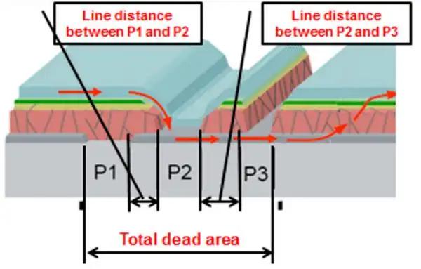
Laser Scribing (P1): Using laser technology to pattern the bottom electrode, isolating individual sub-cells to create series connections.
Functional Layer Coating: Sequentially depositing the electron transport layer (ETL), perovskite absorption layer, and hole transport layer (HTL).
Laser Scribing (P2): Removing the ETL/perovskite/HTL stack to expose the bottom electrode for interconnecting sub-cells.
Top Electrode Deposition: Depositing the top electrode (e.g., metal or conductive oxide).
Laser Scribing (P3): Patterning the top electrode to complete the series connection between sub-cells.
Edge Deletion (P4): Using laser ablation to remove peripheral films (typically 8–15 mm wide) to ensure encapsulation compatibility.
Encapsulation: Sealing the device to protect against environmental degradation.
Laser Applications
1. Ultrafast Laser Processing
Ultrafast lasers (e.g., femtosecond or picosecond lasers) enable cold ablation, minimizing thermal damage to surrounding materials.
Short pulse durations (e.g., 300 fs) reduce the heat-affected zone (HAZ), ensuring precise patterning without compromising adjacent layers.
2. Laser Scribing
P1, P2, and P3 scribing divide the cell into interconnected sub-cells, forming series connections to achieve higher voltage output.
Dead Zone: The non-active scribing region (e.g., P1/P2/P3 lines) should be minimized (<150 μm) to reduce efficiency losses.
Edge Deletion: Removing peripheral films (8–15 mm) prevents short circuits and ensures encapsulation reliability.
3. Advanced Laser Techniques
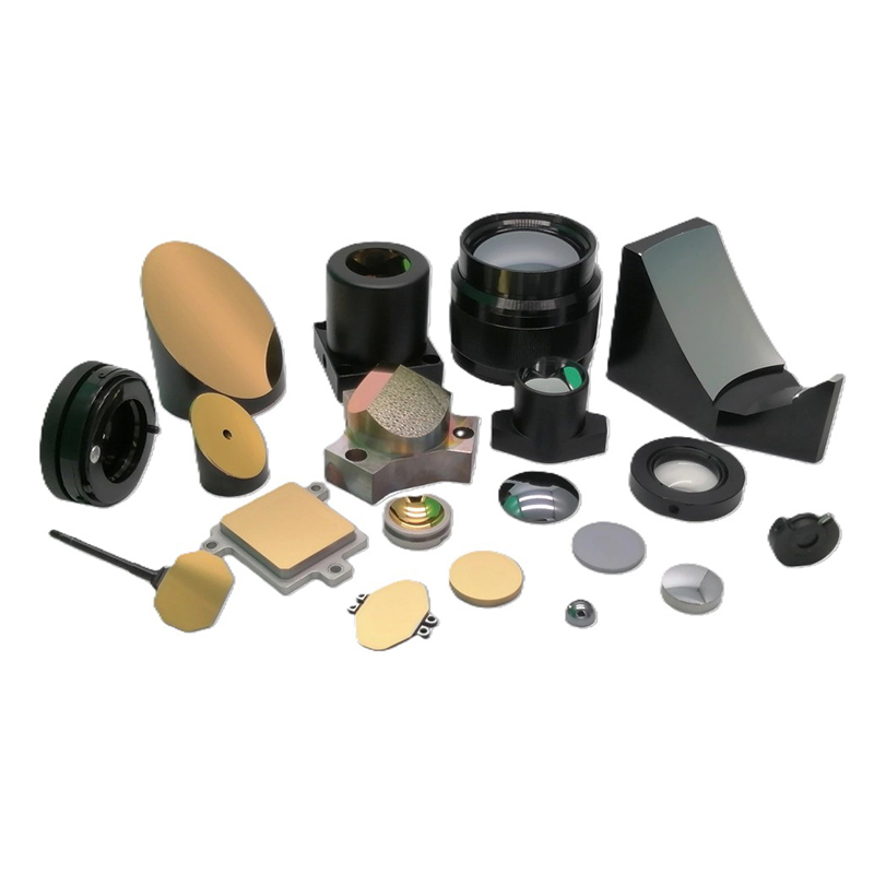
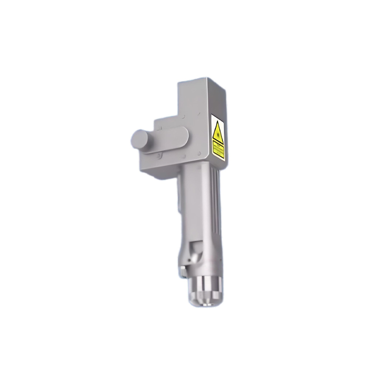
Beam Shaping: Using aspheric lens systems to transform Gaussian beams into flat-top beams, ensuring uniform energy distribution and reducing edge damage.
Dynamic Tracking Systems: Real-time visual tracking and compensation algorithms adjust scribing paths based on the P1 line position, minimizing misalignment and dead zone width.
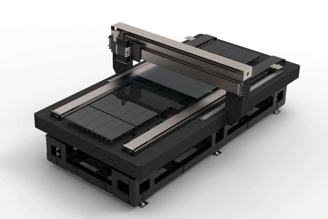
Multi-Beam Processing: GW-scale systems (e.g., 24-beam lasers) enable high-throughput scribing for large-area modules (e.g., 1200 × 2400 mm) with cycle times as low as 30 seconds.
Key Equipment for Perovskite Solar Cells
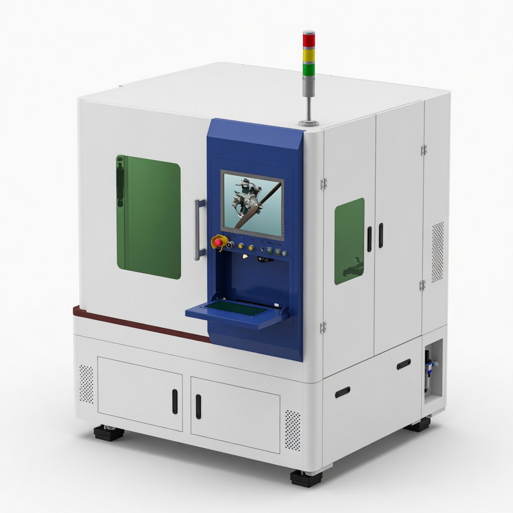
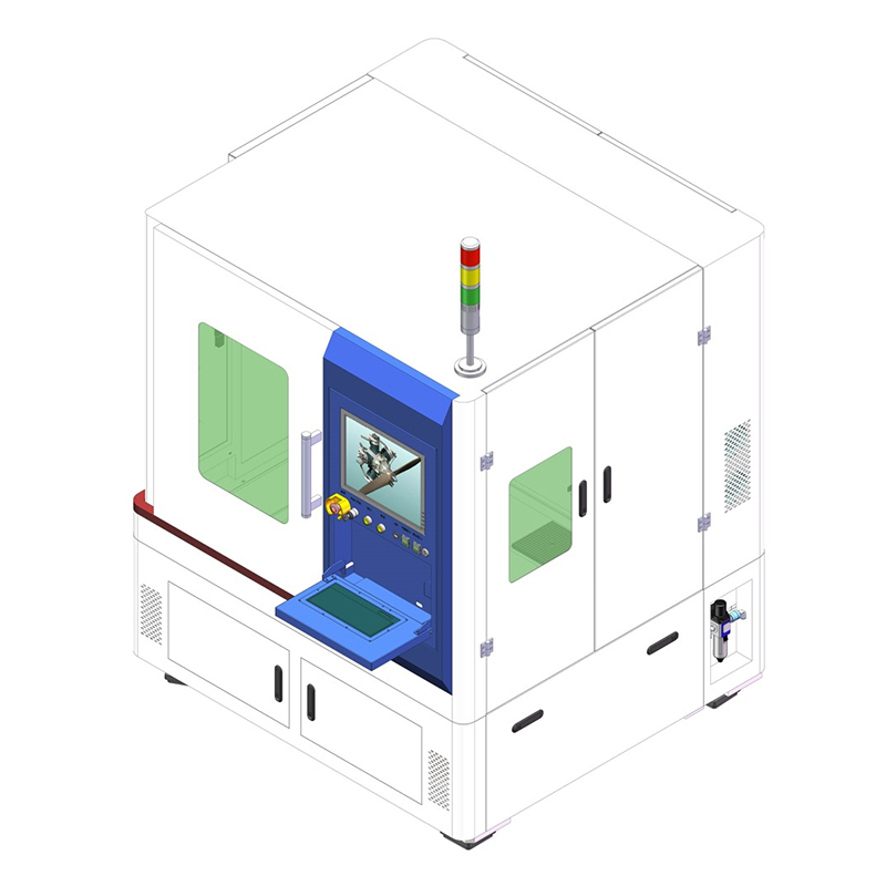
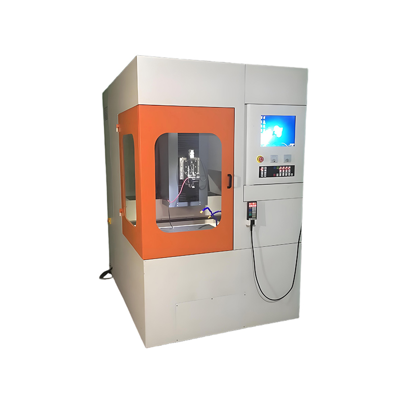
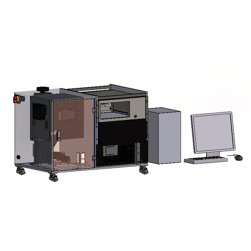
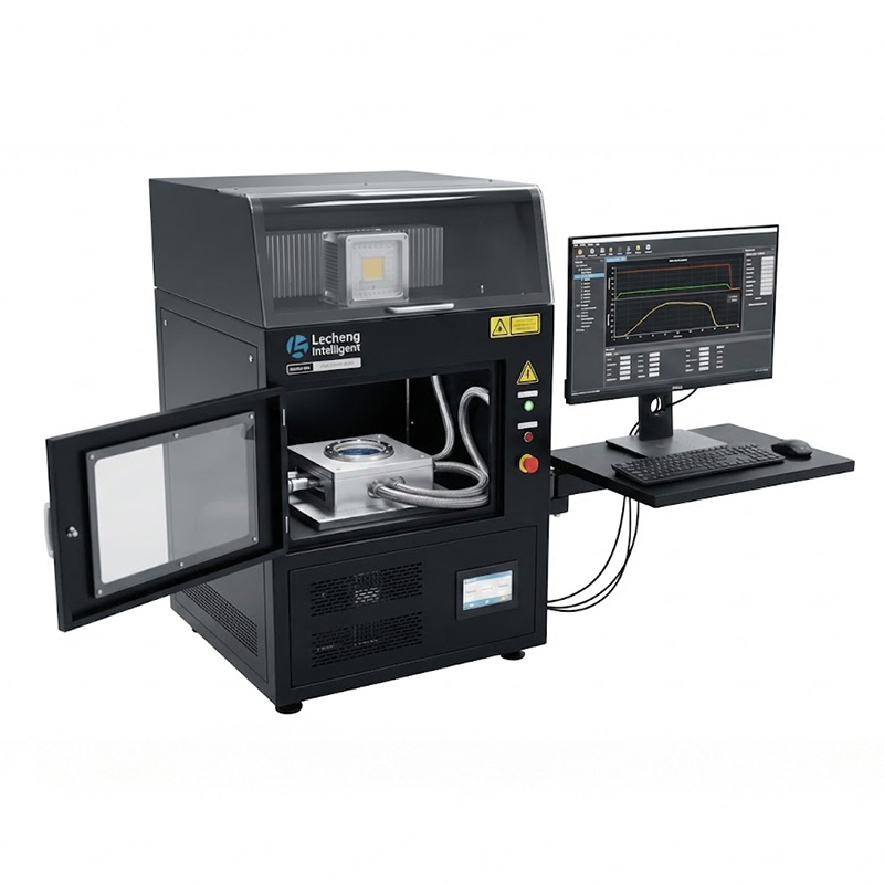
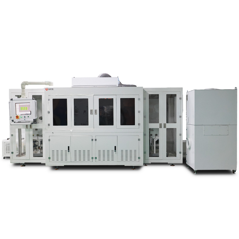
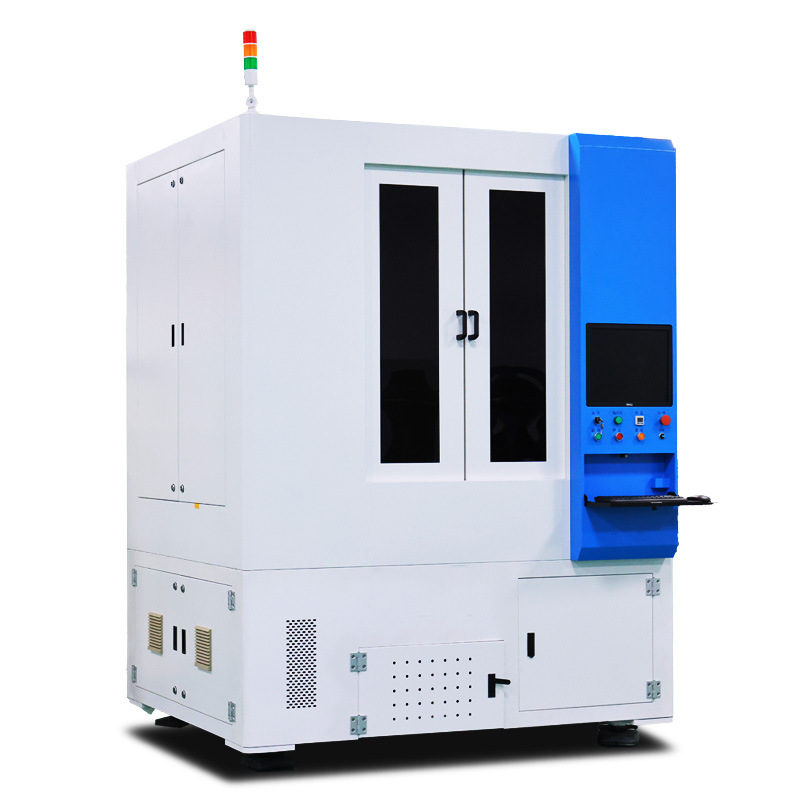
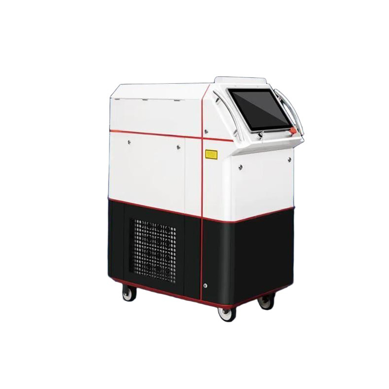
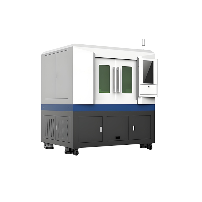
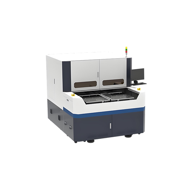
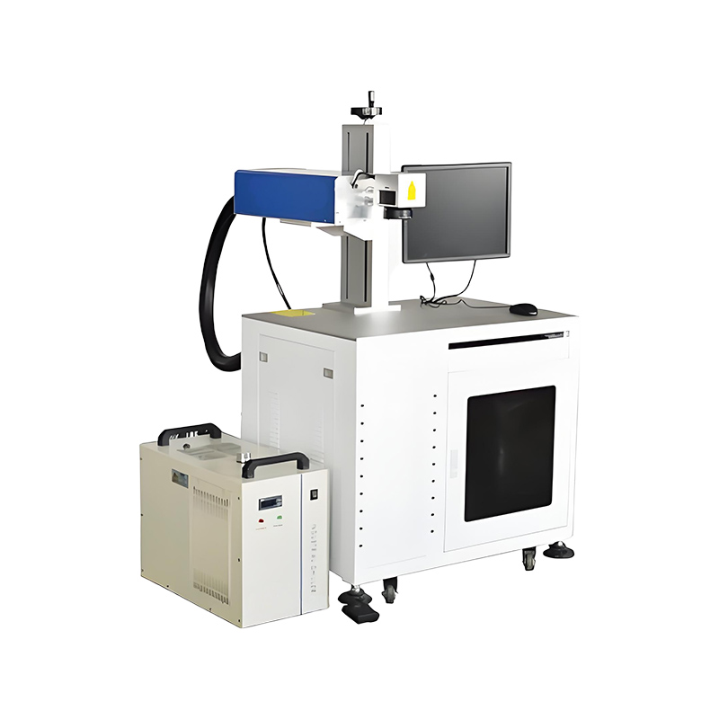
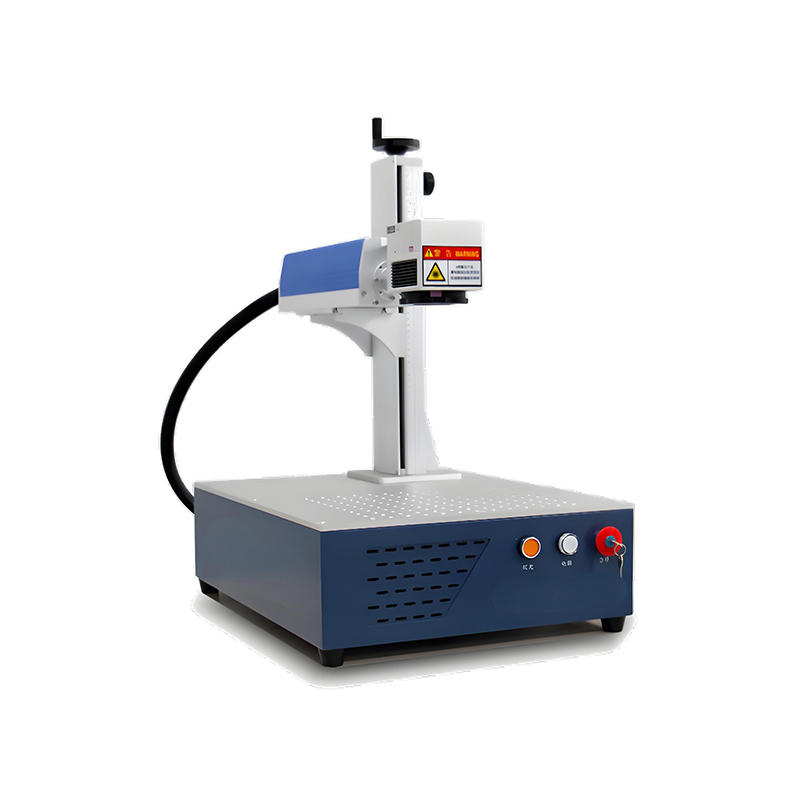
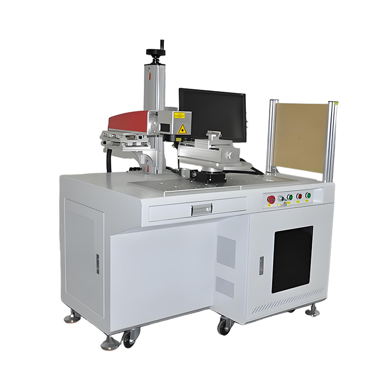
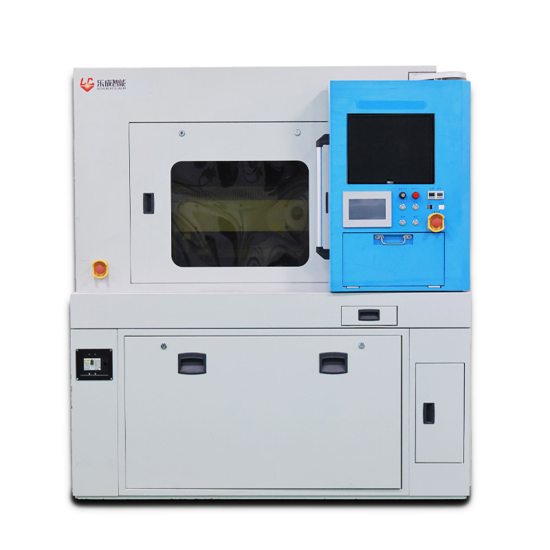
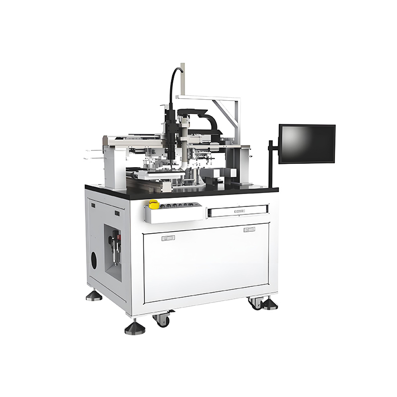
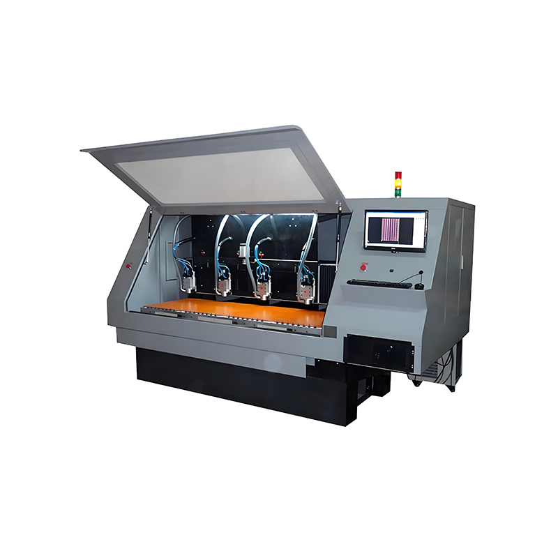
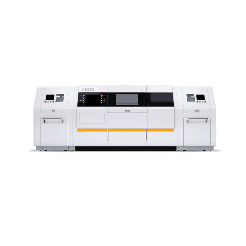
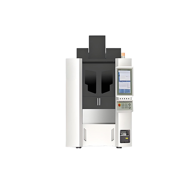
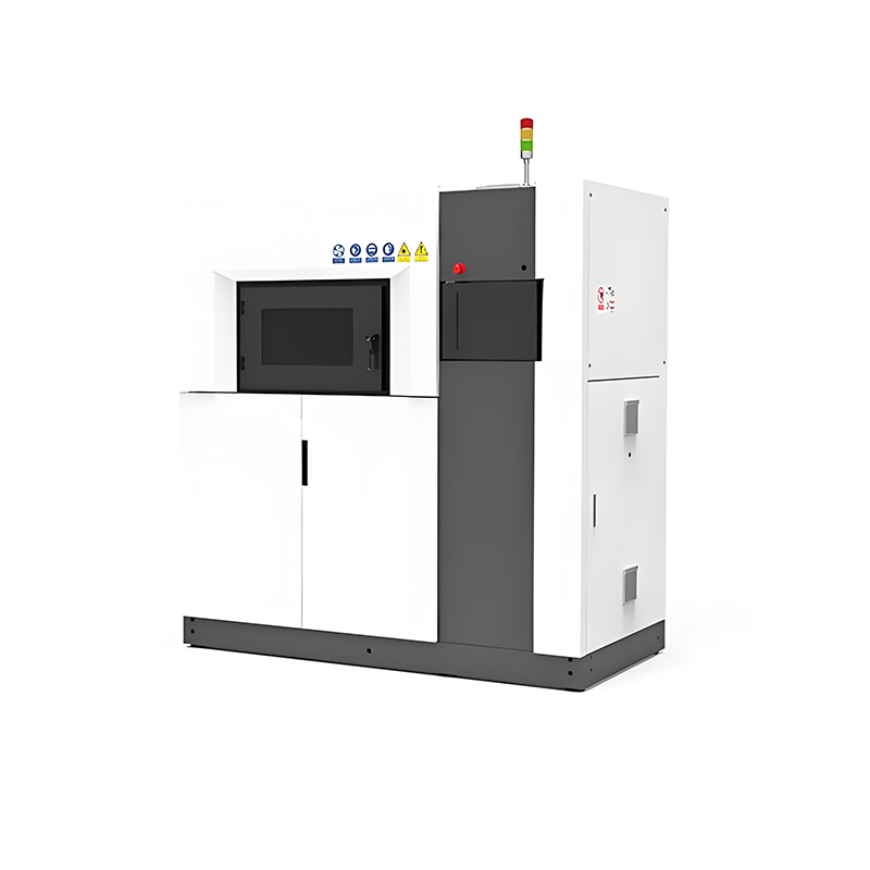
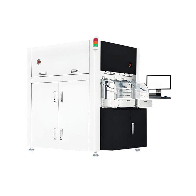
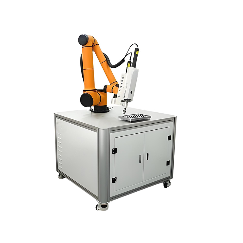
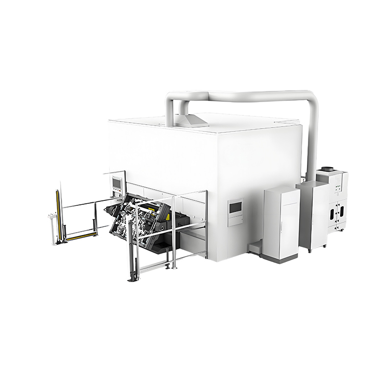
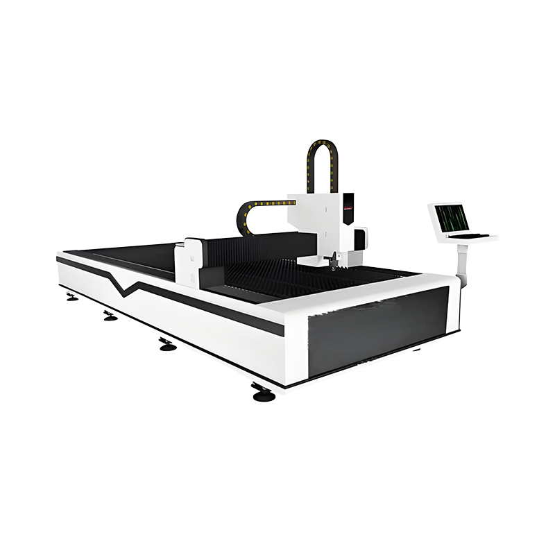
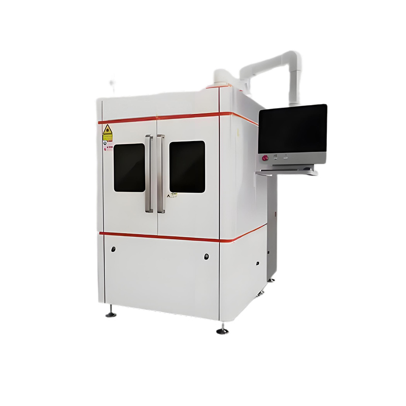
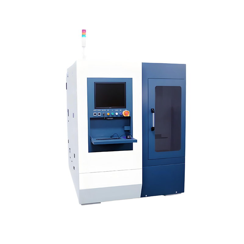
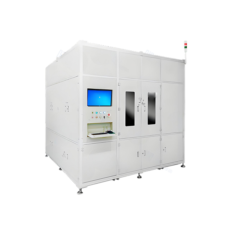
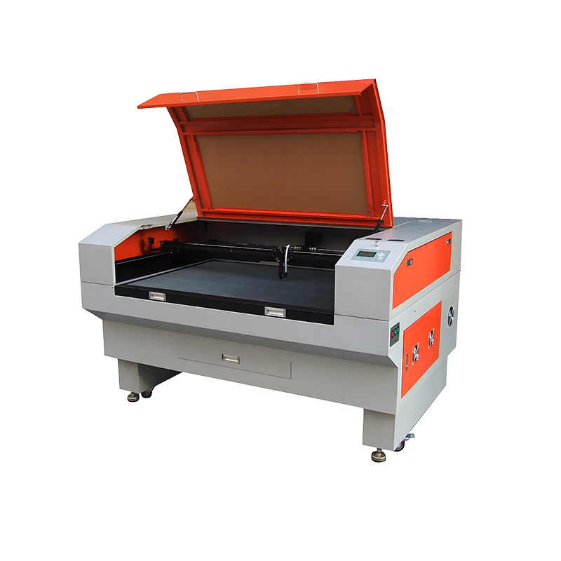
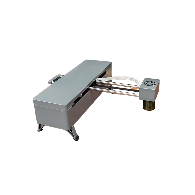
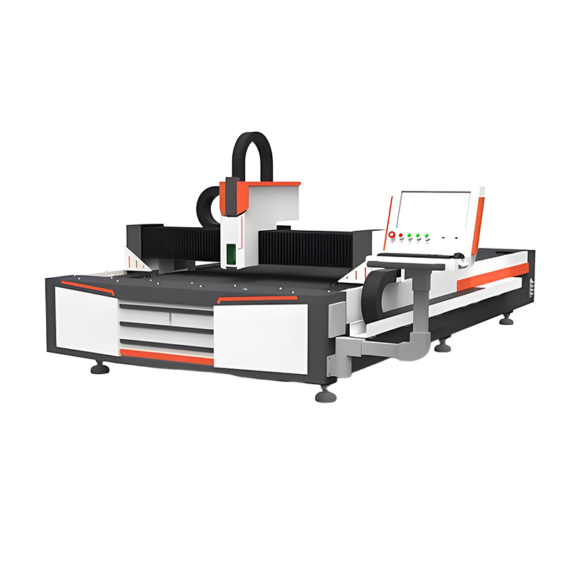
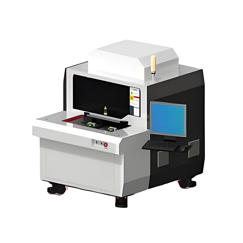
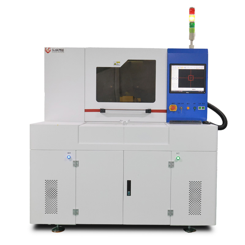
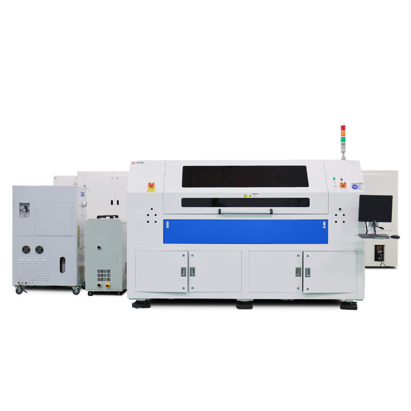
Laser Scribing Systems:
Ultrafast Lasers: Femtosecond/picosecond lasers with wavelengths of 532 nm or 355 nm for precise scribing.
Multi-Beam Optics: Systems with 12–24 independently controlled beams for parallel processing.
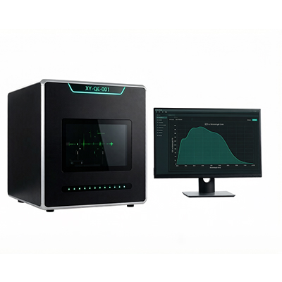
Real-Time Monitoring: Integrated CCD imaging and confocal microscopy to measure scribing depth, width, and defects.
Dynamic Tracking and Compensation:
Sensors detect the P1 line position and automatically adjust P2/P3 paths to maintain consistent spacing (e.g., 10 μm precision).
Benefits: Reduces dead zone width, improves efficiency, and enhances production yield.
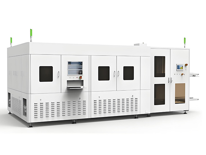
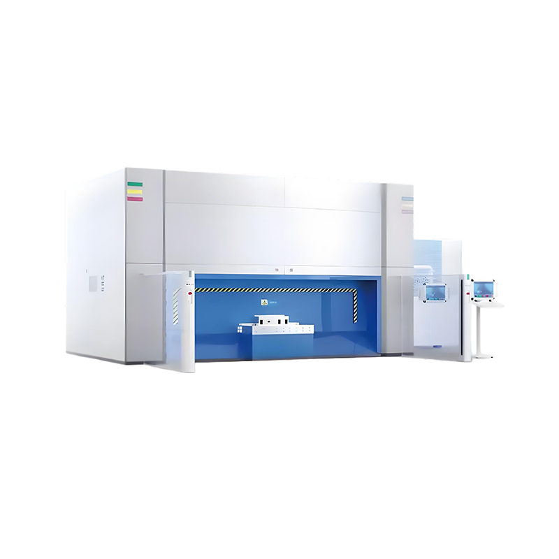
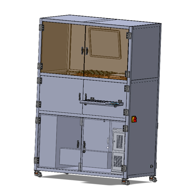
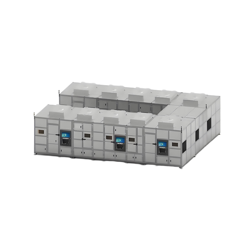
Large-Area Processing Equipment:
GW-scale laser scribing machines (e.g., Qinghong Laser’s system) support modules up to 2.88 m², achieving scribing speeds of 2000–6000 mm/s.
Laser Processing Effects
P1 Scribing
Objective: Completely remove the bottom electrode (e.g., ITO) without damaging the substrate.
Optimized Parameters:
Laser: 532 nm femtosecond laser, 1.8–2.4 W power, 2000 mm/s speed, 1000 kHz frequency.
Result: Scribing width <10 μm, no substrate damage, and minimal HAZ (<1 μm).
P2 Scribing
Objective: Remove the ETL/perovskite/HTL stack to expose the bottom electrode without damaging it.
Optimized Parameters:
Laser: 532 nm femtosecond laser, 0.46 W power, 4000 mm/s speed.
Result: Scribing depth of ~858 nm, precise removal without electrode damage.
P3 Scribing
Objective: Pattern the top electrode (e.g., Au) to isolate adjacent sub-cells.
Optimized Parameters:
Laser: 532 nm femtosecond laser, 0.2 W power, 6000 mm/s speed.
Result: Scribing depth of ~534 nm, no underlying layer damage.
Summary of Advantages
Multi-Beam Processing: 12/24-beam laser systems offer higher stability and independent power control for each beam, improving flexibility and reliability.
Real-Time Focus Tracking: Maintains consistent focal points even on curved or fluctuating substrates, ensuring uniform scribing depth and width.
Visual Tracking and Compensation: Dynamically adjusts P1/P2/P3 spacing to minimize dead zones (<150 μm), enhancing conversion efficiency and production yield.
Scalability: GW-scale equipment enables large-area module production (e.g., 2.88 m²) with high throughput (30-second cycle times).
SEO Keywords
Core Keywords:
Perovskite solar cell laser scribing
Ultrafast laser processing perovskite
P1 P2 P3 laser patterning
Dead zone reduction perovskite solar cells
Large-area perovskite module manufacturing
Long-Tail Keywords:
Femtosecond laser scribing for perovskite batteries
Dynamic tracking system laser patterning
Multi-beam laser scribing equipment
GW-scale perovskite laser processing
Laser edge deletion encapsulation perovskite
This overview highlights the critical role of laser technology in advancing perovskite solar cell efficiency, scalability, and commercialization. For specific technical details or equipment recommendations, consult specialized manufacturers like Qinghong Laser or Yuanlu Photonics.

