Application of LIDE Laser-Induced Deep Etching Technology in MEMS Packaging
With the continuous innovation of MEMS technology, MEMS devices are widely used in consumer electronics, medical equipment, and aerospace applications, offering significant value due to their compact size, high speed, reliability, and low cost. MEMS packaging is a critical step in MEMS device development. MEMS (Micro-Electro-Mechanical Systems) packaging involves the process of sealing and protecting MEMS devices, providing electrical connections while shielding the device from environmental influences. The packaging process can account for 20% to 95% of the product’s manufacturing costs.
01 Glass as a Preferred Material for MEMS Manufacturing
Innovations in glass wafer processing technology are driving advancements in MEMS technology. Glass wafers are used in MEMS wafer-level packaging and serve as an alternative substrate to silicon wafers in certain electronic products. MEMS sensors demonstrate high reliability and long-term performance even in harsh environments. Glass materials are commonly used as substrate carriers in MEMS packaging technology, making glass wafers an ideal choice for various industries and applications.
02 Advantages of Glass in MEMS Manufacturing and Packaging
Glass is a preferred material for MEMS packaging due to its high airtightness, thermal stability, optical properties, chemical resistance, high insulation, and machinability. Its durability ensures long-term protection for MEMS devices.
Optical Properties
Glass is transparent, making it ideal for MEMS devices requiring optical sensing or actuation. It can be coated with various thin-film materials, such as metals or oxides, to modify its optical properties. Additionally, its highly smooth surface is an excellent choice for optical reflection.
Encapsulation and Packaging
High Airtightness: Glass provides excellent hermetic sealing, preventing moisture and other contaminants from entering MEMS devices, thereby enhancing reliability and lifespan.
Exceptional Chemical Resistance: Glass is highly resistant to chemical corrosion, making it an excellent material for protecting MEMS devices in harsh chemical environments.
Mechanical Strength: Glass is relatively robust and durable, protecting MEMS devices from mechanical stress. Unlike metals or other materials, glass does not suffer from fatigue effects, making it suitable for long-term high-reliability applications.
Unlike silicon, glass is highly insulating, and its coefficient of thermal expansion (CTE) and mechanical strength can be adjusted within a certain range.
Interconnection with Through-Glass Vias (TGV)
Higher-Density Interconnections: TGV enables high-density interconnections, allowing for more complex MEMS devices and smaller form factors. This is due to the high aspect ratio of TGV vias, which facilitate vertical interconnections through the glass substrate.
Improved Reliability: TGV provides more reliable interconnections compared to wire bonding or flip-chip bonding. The shorter path length of TGVs reduces signal delay and electromagnetic interference (EMI).
Thermal Stability: TGVs efficiently dissipate heat from MEMS devices by conducting it through the glass substrate to the exterior of the package. This significantly improves the thermal management of MEMS devices and extends their lifespan.
Flexibility in Packaging: TGVs are compatible with various interconnection methods, offering greater flexibility in MEMS packaging design. This enables the integration of more sensors, actuators, and other components into a single package.
Enhanced Optical Performance: TGVs can be mass-produced with small diameters, enabling integration with optical fibers or other optical components. This facilitates the combination of MEMS devices with optical sensing or actuation functions.
03 German LPKF LIDE Process Significantly Improves Thin Glass Processing Efficiency
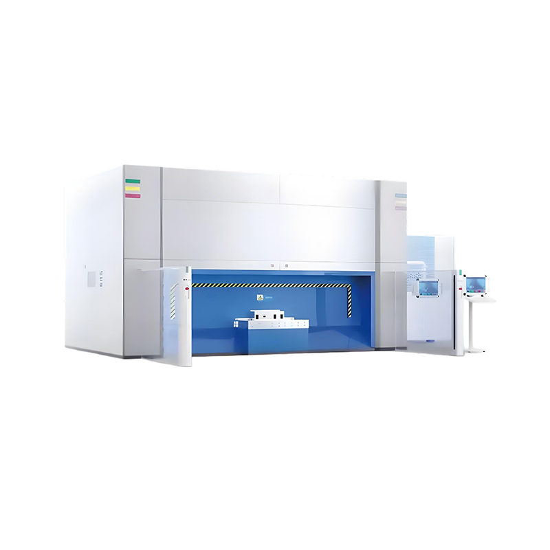
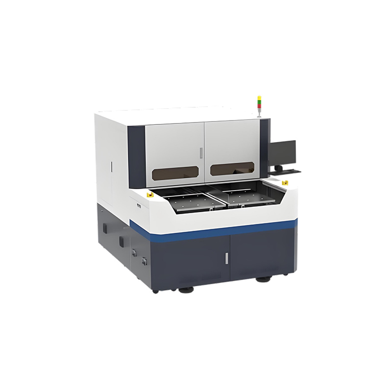
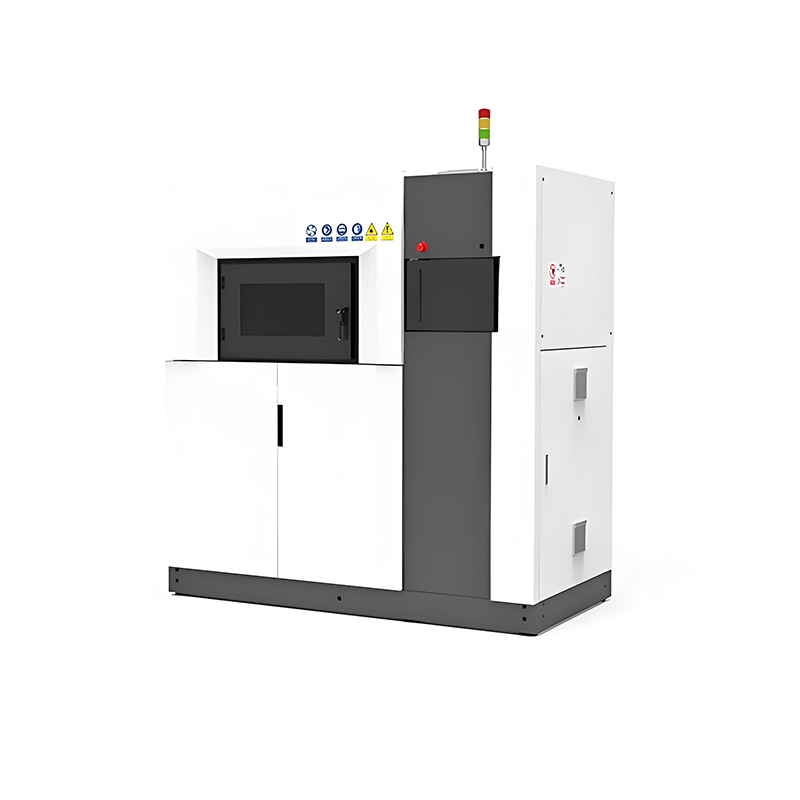
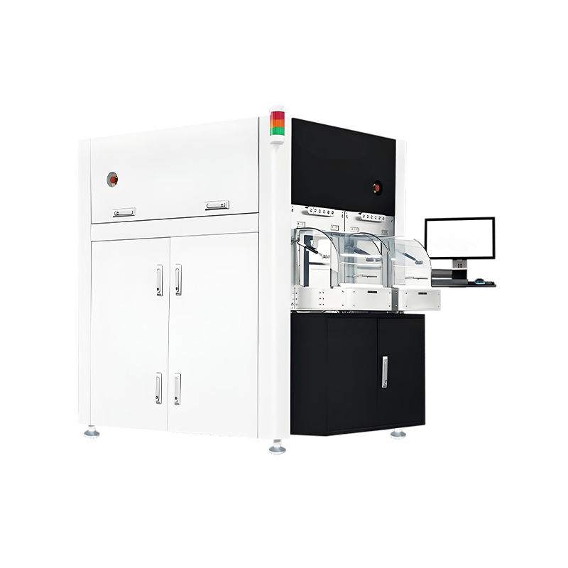
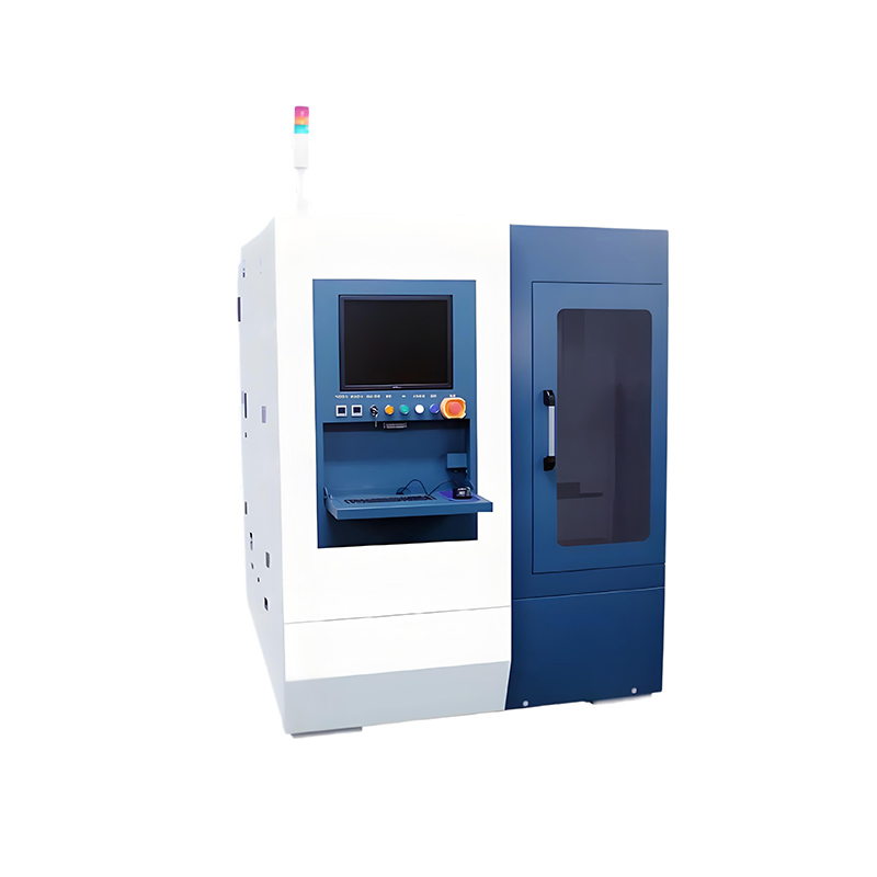
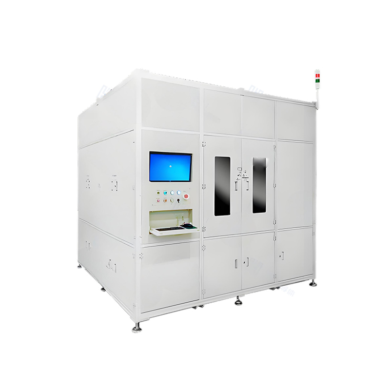
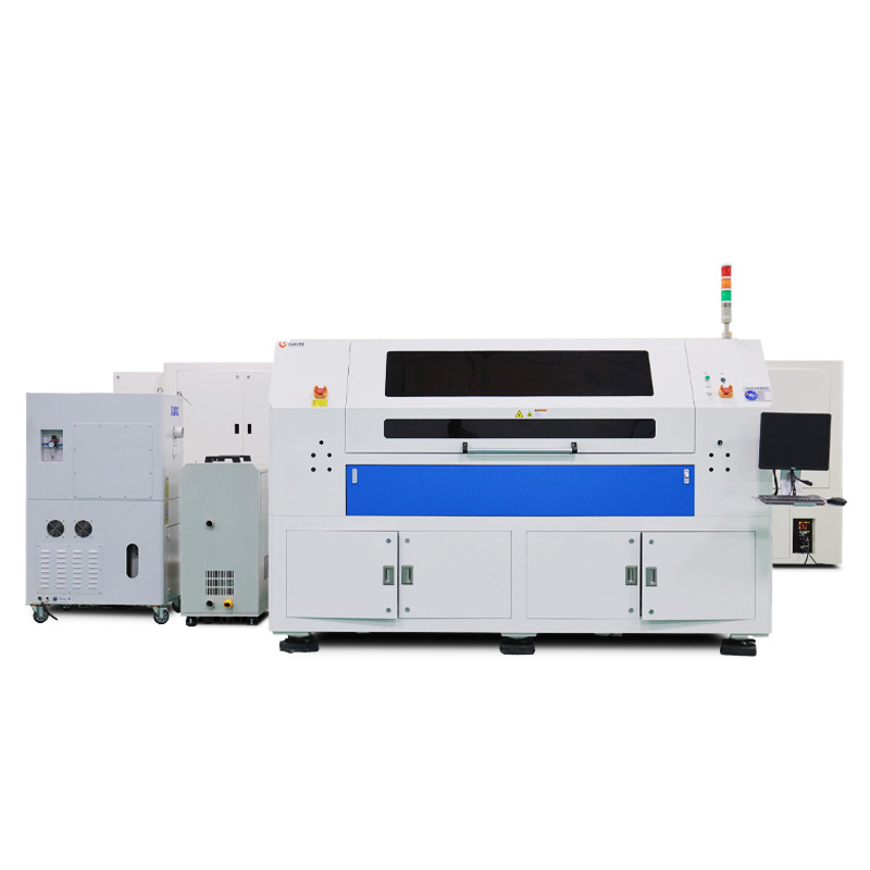
Thin glass sheets ranging from 50 μm to 1,000 μm hold great potential for various industrial applications. However, traditional mechanical cutting and drilling processes often leave micro-cracks and residual internal stresses in glass substrates, making thin glass challenging to process at a micro-scale. The LPKF Vitrion laser system, utilizing the latest LIDE (Laser-Induced Deep Etching) technology, enables non-contact precision laser processing of glass materials with unprecedented efficiency and quality. The LIDE process unlocks new design possibilities in microsystems and has the potential to revolutionize the entire industry chain.
The LIDE technology requires only two steps to address these challenges:
Selective Laser Modification: Based on the design pattern, the glass is selectively modified using a specially developed laser source. The laser is focused inside the glass component, achieving full-thickness modification.
Chemical Etching: The laser alters the photochemical properties of the material, allowing for selective chemical etching in the subsequent process. The etching rate of the modified areas is significantly higher than that of unmodified material. The time the glass spends in the etching bath is precisely controlled to achieve the desired structural dimensions.
04 Applications of LPKF LIDE in MEMS
The LIDE process enables the creation of defect-free glass-based microsystems that retain the high fracture strength of the original material while exhibiting high "elasticity" with excellent repeatability. This capability allows for the integration of structures such as springs, vertical or horizontal membranes, and actuation or sensing components.
Force-Displacement Sensing Measurements:
LIDE-processed glass spring systems.
Micro-spring structures with a cross-section of 30 μm × 260 μm and an X-Y platform size of 5 mm × 7 mm.
The X-Y system has a Z-axis displacement range of up to 4.3 mm.
High repeatability and a fracture strength of approximately 1 GPa.
Radial Comb Drive Optical Reflection Measurements:
Two glass wafers with microstructures and sputtered metal films are stacked together.
Comb structures with a gap width of 5 μm.
Piezoelectrically driven optical reflection systems achieve out-of-plane angular deflection of ±3.1° at 220 Hz.
Optical reflection area of 7 mm × 7 mm.
Core SEO Keywords
LIDE laser etching
MEMS packaging technology
Through-Glass Via (TGV)
Glass substrate MEMS
Laser-induced deep etching
Hermetic packaging MEMS
Ultra-thin glass processing
LPKF Vitrion system
MEMS sensors reliability
Glass interposers MEMS

