Why Precision Laser Processing is Key to Higher Perovskite Module Efficiency
The Direct Path to Maximizing Active Area
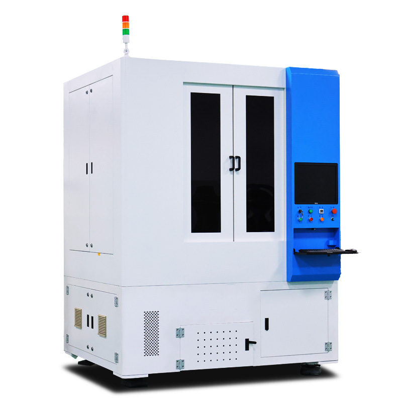
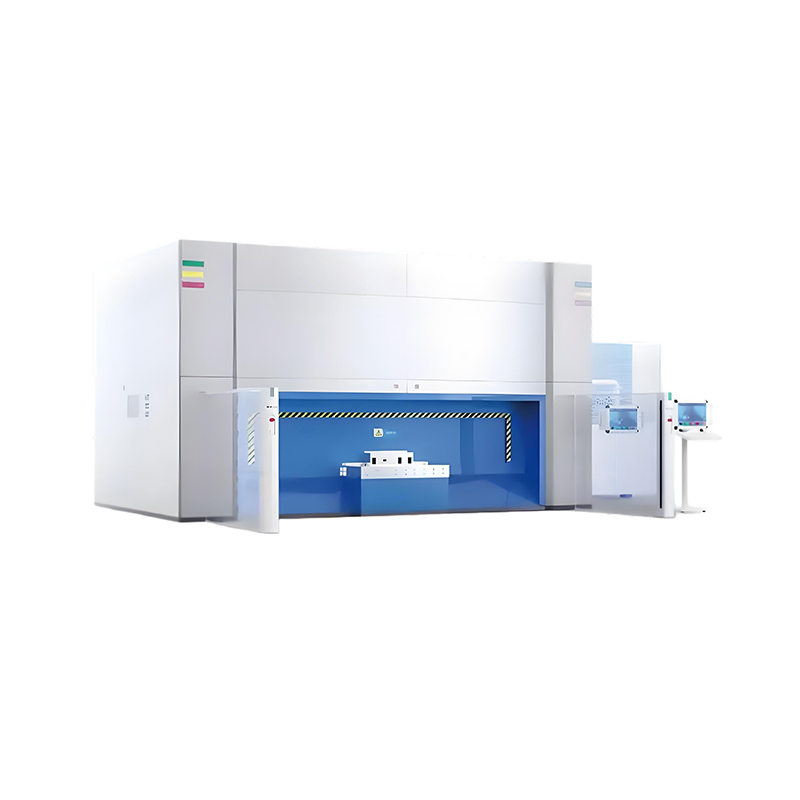
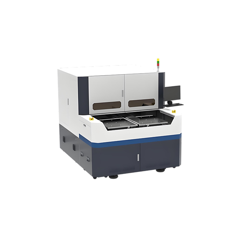
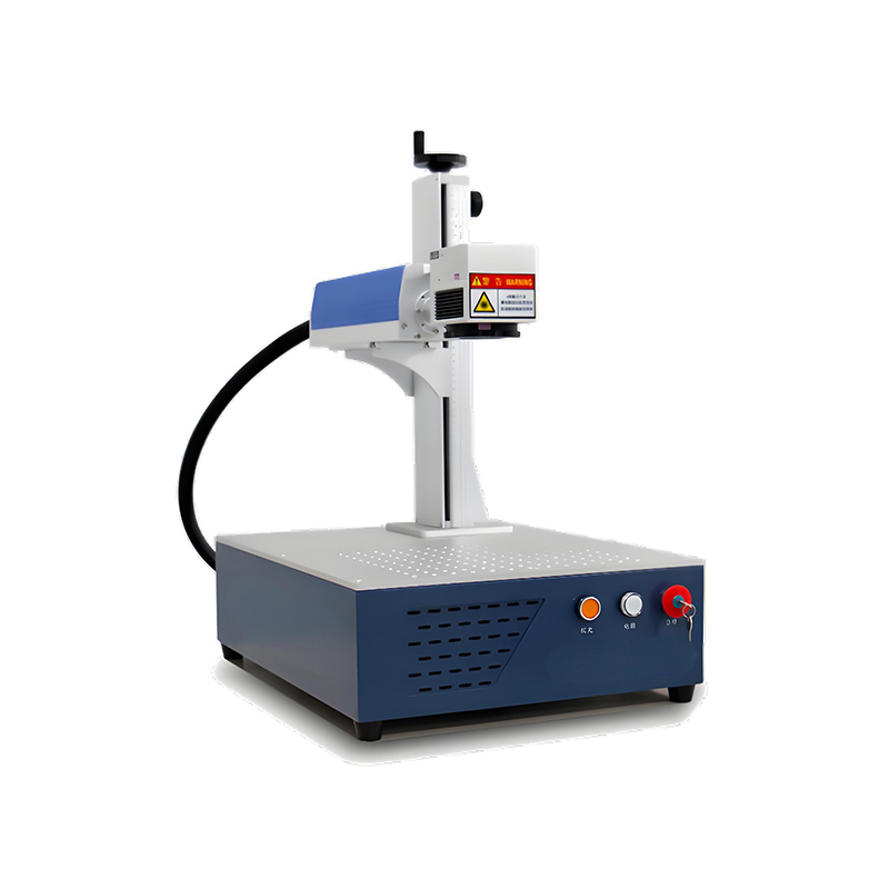
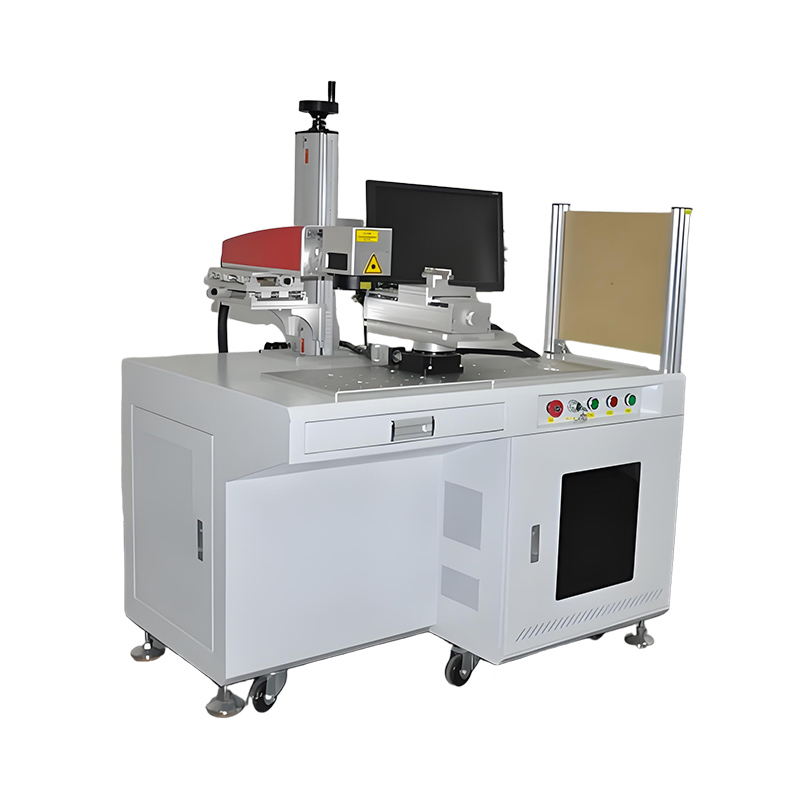
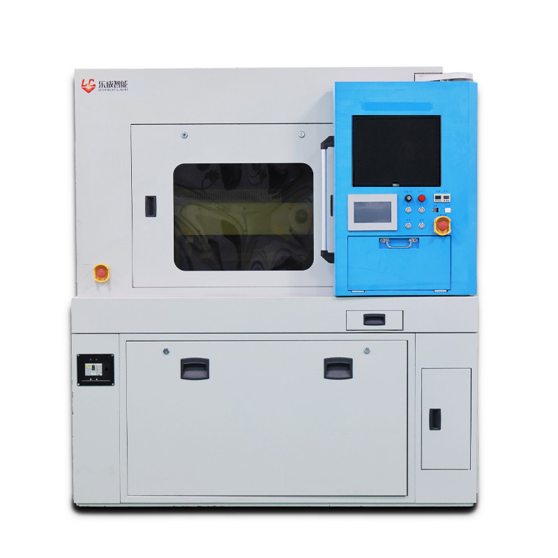
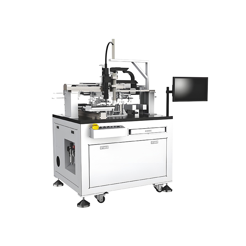
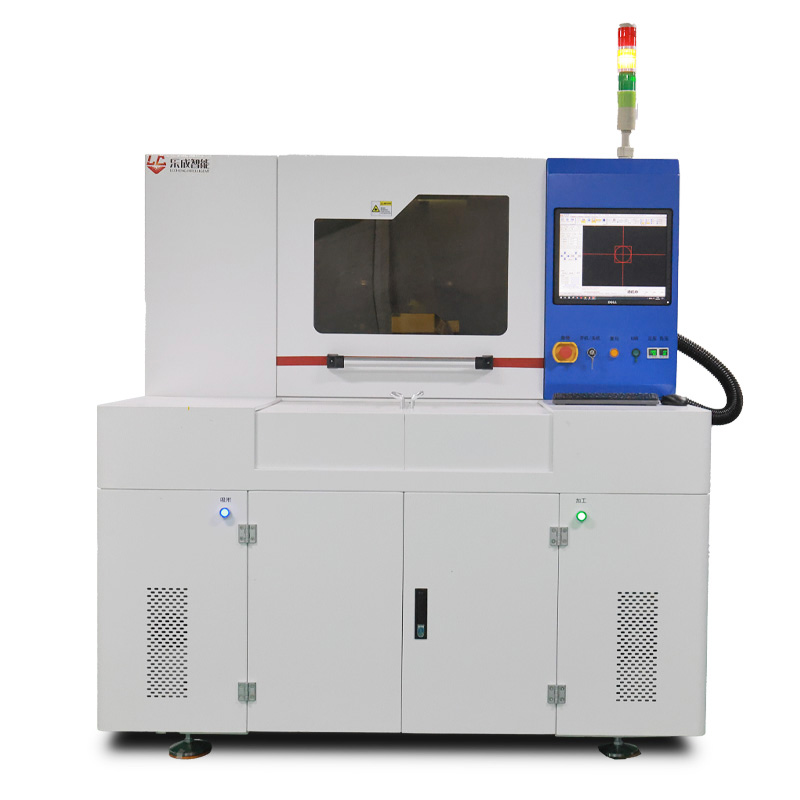
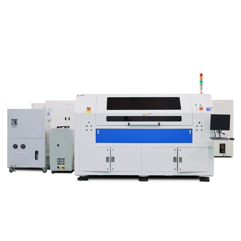
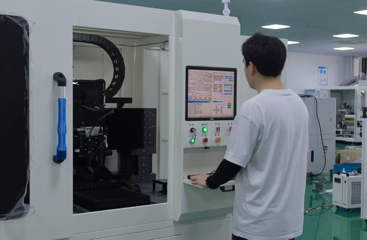
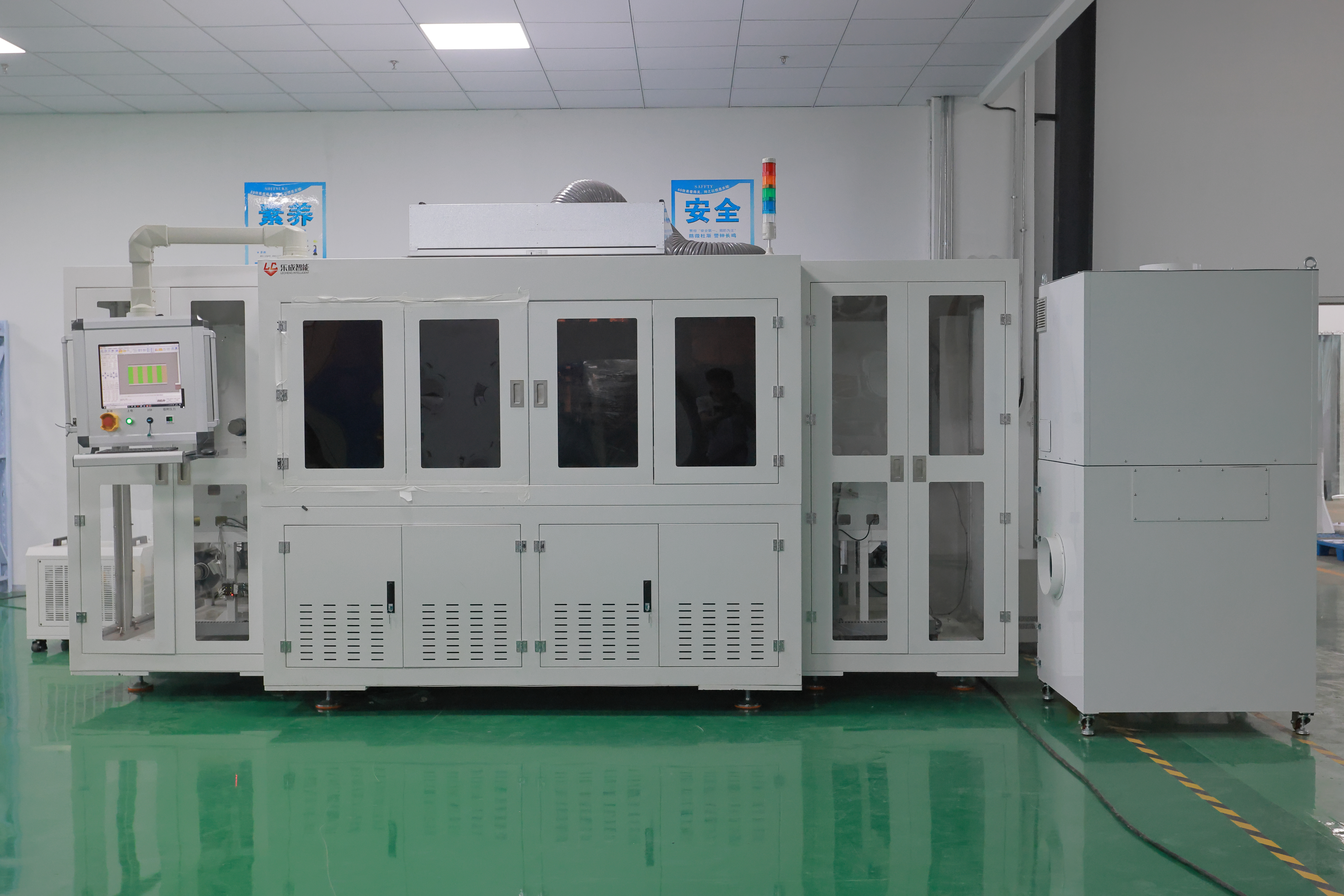
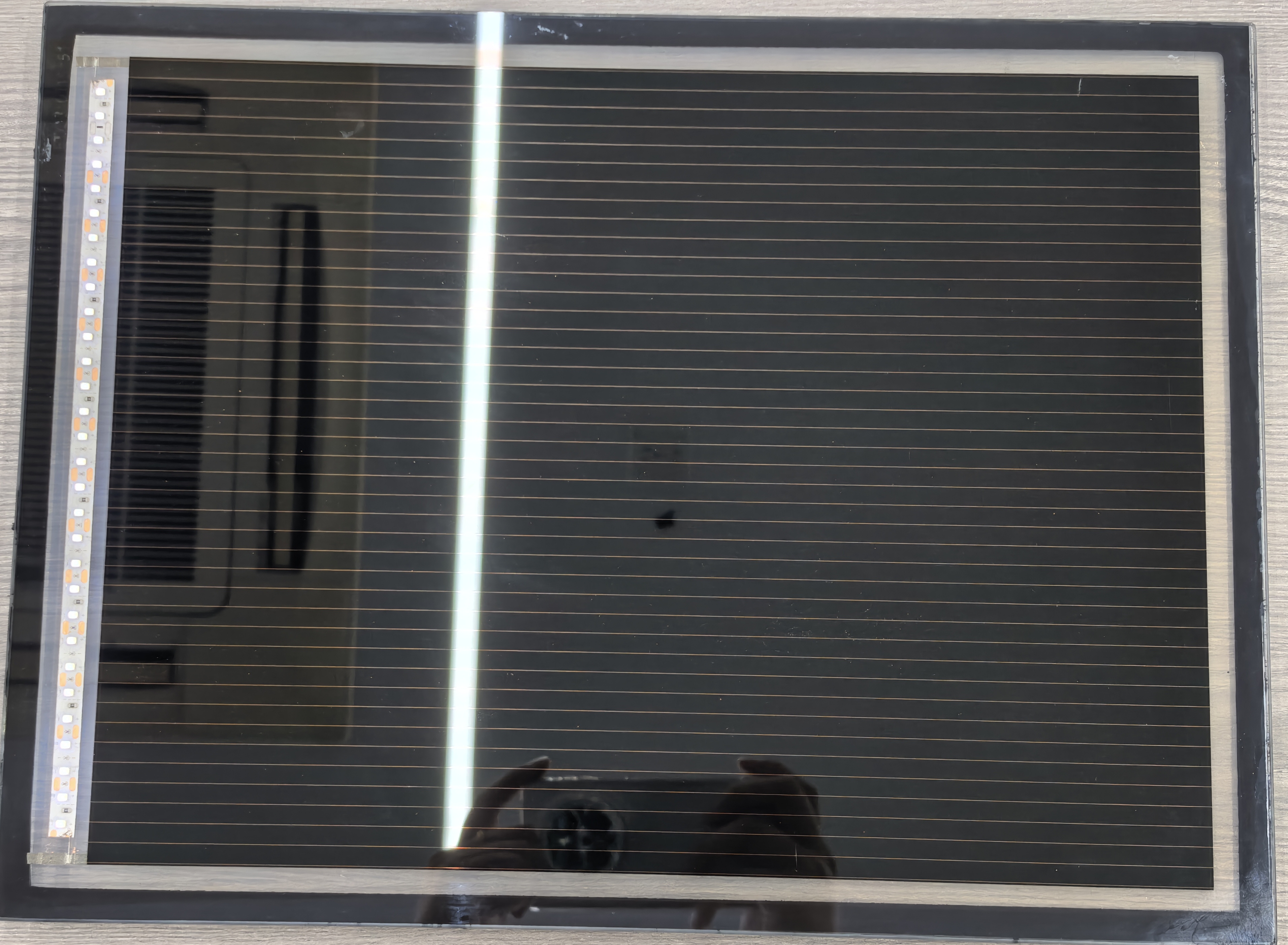
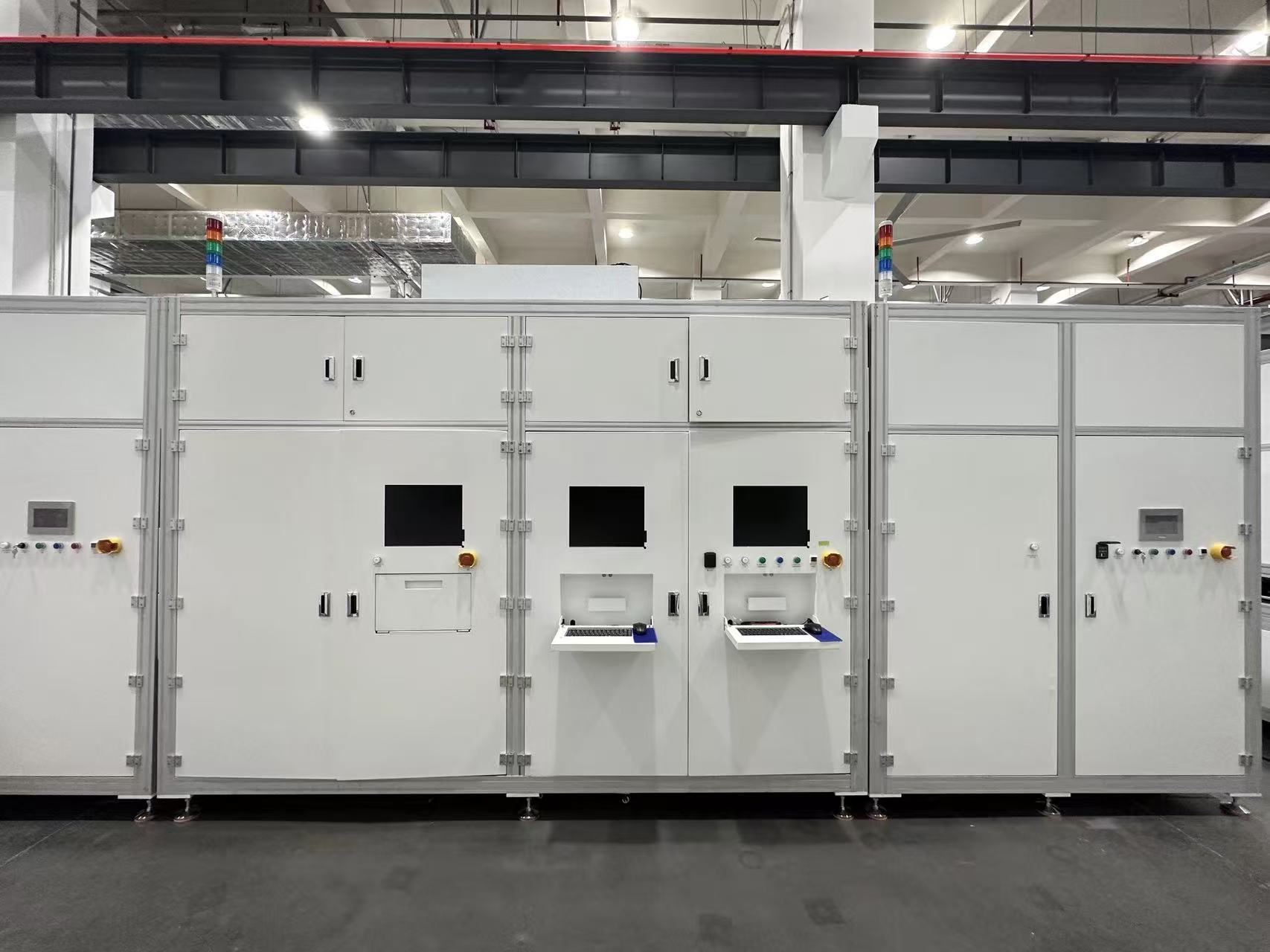
The fundamental principle for achieving high efficiency in any solar module is to maximize the area that converts sunlight into electricity, known as the active area. In perovskite solar cells, this is critically dependent on the laser scribing processes—P1, P2, and P3—which isolate and interconnect individual cell strips to form a series-connected module. The space occupied by these scribed lines is called the "dead zone," as it does not contribute to power generation. Lecheng Intelligent's precision laser systems are engineered specifically to minimize this dead zone. Their technology achieves remarkably narrow scribe lines with widths below 30μm and exceptional straightness with a positional accuracy of ±5μm. More importantly, Lecheng's advanced Trajectory Tracking software plays a pivotal role. It intelligently scans the actual path of the P1 line and then adjusts the paths for the P2 and P3 scribes to follow this trajectory precisely. This ensures the minimal necessary gap between lines is maintained consistently, even if the P1 line has minor curvatures. Without this technology, manufacturers are forced to increase the spacing between lines to account for potential misalignment, unnecessarily widening the dead zone and reducing the active area. By enabling tighter, more accurate scribe patterns, Lecheng's laser processing directly increases the module's active area, which is a primary factor in boosting overall power output and efficiency.
The Role of Ultra-Low Thermal Impact
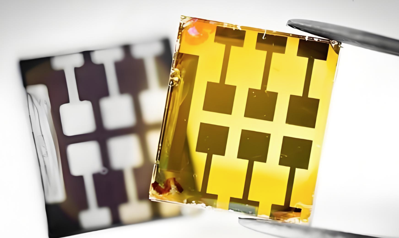
The efficiency of a perovskite solar cell is not solely determined by its size but also by the quality of the materials within the active area. Traditional mechanical scribing or less precise laser methods can cause significant damage to the delicate multi-layer structure of a perovskite cell, leading to shunts or reduced performance in the areas adjacent to the scribe lines. Lecheng Intelligent addresses this challenge through the use of ultra-short pulse lasers (picosecond and femtosecond) and sophisticated optical control. These lasers deliver energy in incredibly short bursts, vaporizing the target material with minimal heat transfer to the surrounding layers. This results in an exceptionally small Heat-Affected Zone (HAZ). For instance, Lecheng's processes can achieve a HAZ of less than 1μm for the P2 scribe, which is critical when etching through the hole transport, perovskite, and electron transport layers without damaging the underlying TCO layer by more than 20% of its thickness. Clean, defect-free scribes with minimal HAZ prevent current leakage and ensure that each individual sub-cell operates at its peak performance. This meticulous preservation of the functional materials around the scribes ensures that the generated electrical current is efficiently collected and that the voltage of the series-connected cells is maximized, directly contributing to a higher module conversion efficiency.
Enabling Scalability and Reproducibility for Commercial Viability
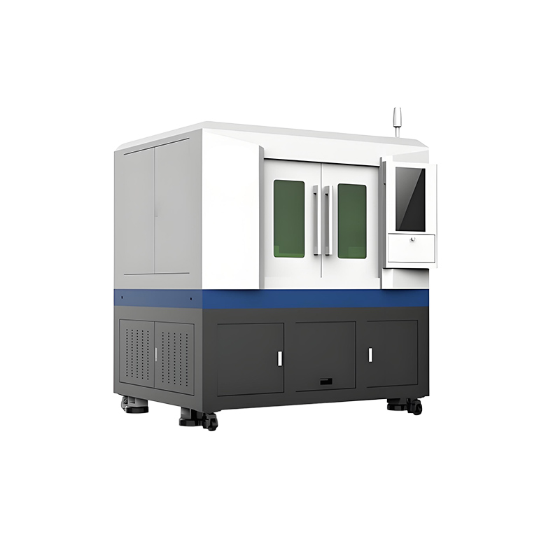
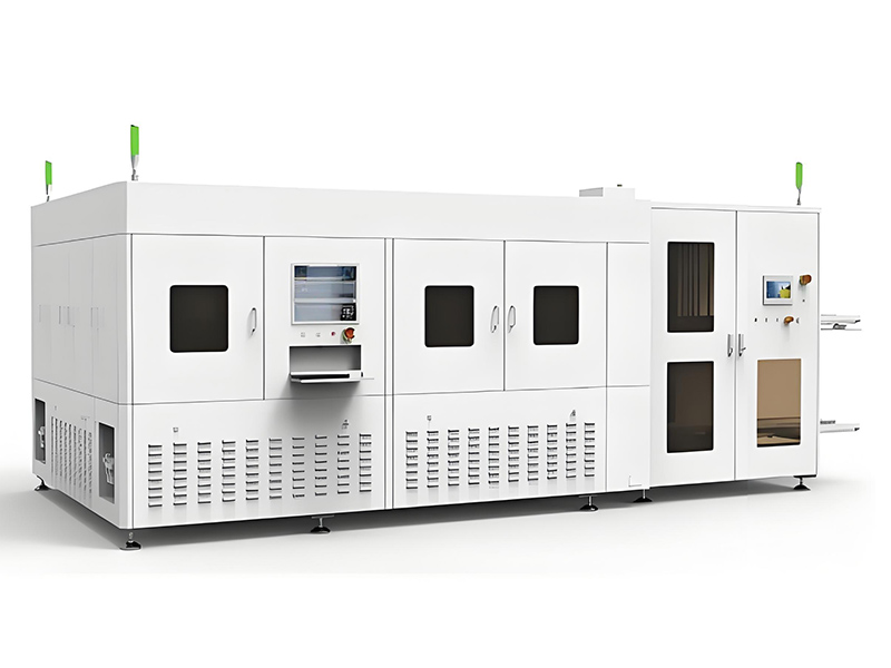
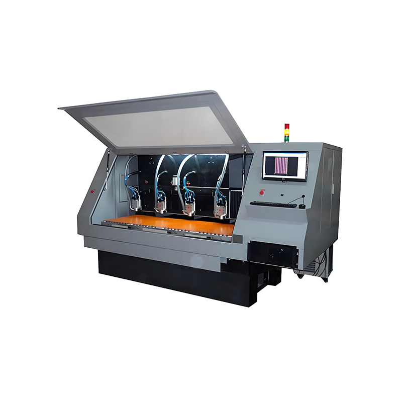
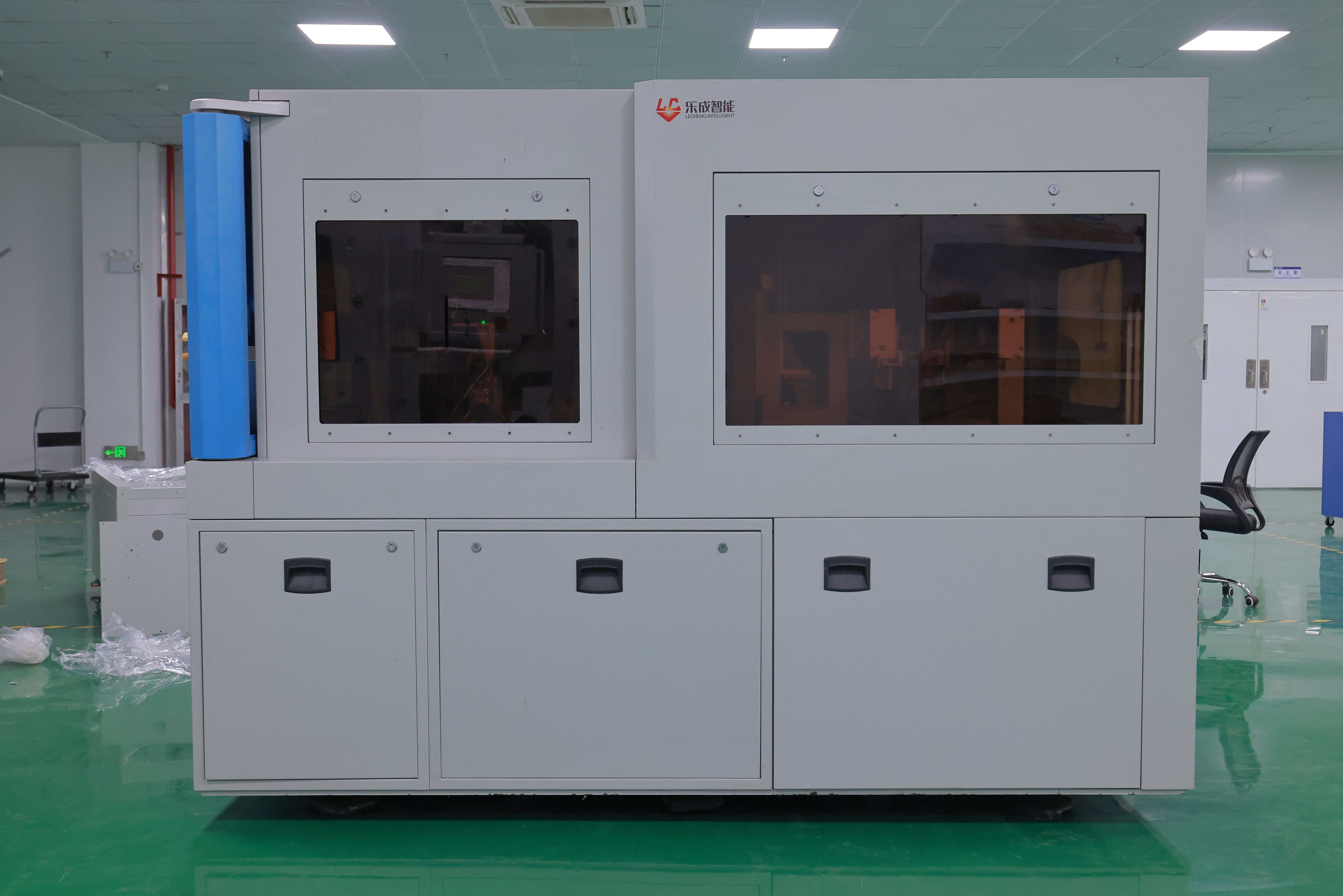
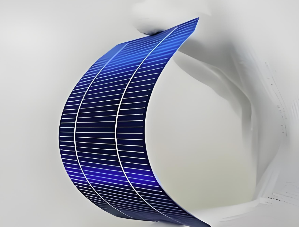
For perovskite technology to transition from lab-scale champions to commercially viable products, manufacturing processes must be not only precise but also highly repeatable and scalable to large panel sizes. Inconsistencies in scribing depth, width, or alignment across a large area (e.g., 2.4m x 1.2m) directly lead to variations in cell performance, creating "hot spots" or reducing the output of the entire module, which is limited by its weakest cell. Lecheng Intelligent's laser systems incorporate Focus Following technology, which uses sensors to continuously monitor the height of the glass substrate and dynamically adjust the laser's focal point in real-time. This compensates for any substrate warping or stage flatness issues, guaranteeing consistent scribing quality across the entire panel. Furthermore, their capability for multi-beam processing (up to 24 beams) allows for high-throughput manufacturing without sacrificing precision. This combination of large-format handling, active focus control, and parallel processing ensures that every square centimeter of a perovskite module, whether in the center or at the edge, receives the same high-quality laser treatment. This reproducibility is essential for achieving high manufacturing yield and stable, reliable module performance in a gigawatt-scale factory, making precision laser processing not just a technical step, but a cornerstone of the entire commercialization effort for perovskite photovoltaics.

In the race to commercialize high-efficiency perovskite solar modules, precision laser processing is not merely an optional manufacturing step; it is a fundamental enabler. By minimizing dead zones, preserving material integrity with ultra-low thermal impact, and ensuring reproducibility across large areas, companies like Lecheng Intelligent are providing the essential tools to unlock the full potential of this promising technology. The path to higher module efficiency is, quite literally, being carved by laser light.

