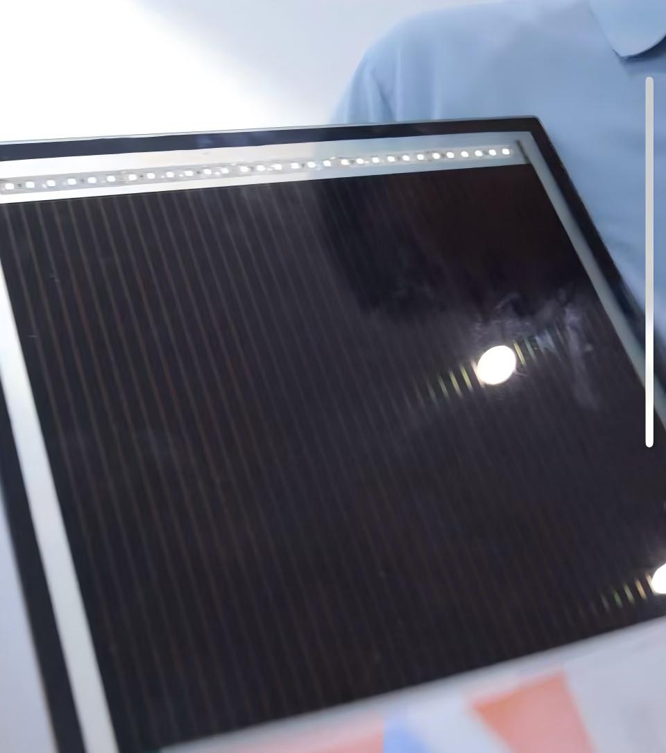
The rapid expansion of the Internet of Things (IoT) has created an urgent need for sustainable power sources for wireless sensor networks and portable electronic devices. This article presents recent breakthroughs in flexible thin-film silicon photovoltaic modules fabricated on polyimide substrates, which demonstrate exceptional performance under indoor lighting conditions. Through optimized plasma-enhanced chemical vapor deposition (PECVD) processes and strategic material engineering, these lightweight, bendable solar modules achieve remarkable 9.1% aperture efficiency at 300 lux illumination while maintaining mechanical robustness through thousands of bending cycles. The technology offers a promising solution for powering the next generation of autonomous electronic devices without battery replacement constraints.The rapid expansion of the Internet of Things (IoT) has created an urgent need for sustainable power sources for wireless sensor networks and portable electronic devices. This article presents recent breakthroughs in flexible thin-film silicon photovoltaic modules fabricated on polyimide substrates, which demonstrate exceptional performance under indoor lighting conditions. Through optimized plasma-enhanced chemical vapor deposition (PECVD) processes and strategic material engineering, these lightweight, bendable solar modules achieve remarkable 9.1% aperture efficiency at 300 lux illumination while maintaining mechanical robustness through thousands of bending cycles. The technology offers a promising solution for powering the next generation of autonomous electronic devices without battery replacement constraints.
1 Introduction: The Indoor Photovoltaics Revolution
The proliferation of IoT devices and wireless sensor networks has highlighted the limitations of battery power sources, which require periodic replacement and create environmental waste. Indoor photovoltaics (IPV) represents a transformative approach to energy harvesting, converting ambient light from artificial sources into continuous electrical power. While conventional solar cells are optimized for outdoor conditions, IPV requires specialized materials and architectures capable of efficient operation under low-intensity, spectrally-limited indoor lighting.
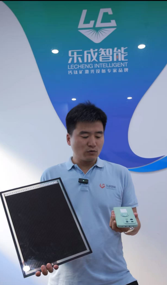
Flexible hydrogenated amorphous silicon (a-Si:H) thin-film solar cells have emerged as particularly suitable for IPV applications due to their high absorption coefficient in the visible spectrum, compatibility with low-temperature processing on plastic substrates, and proven stability under indoor lighting conditions. Recent advancements in deposition techniques and interface engineering have enabled significant improvements in power conversion efficiency, making a-Si:H modules increasingly competitive for practical IoT applications.
2 Materials and Manufacturing Innovations
2.1 Advanced PECVD Process Optimization
The performance of a-Si:H solar cells critically depends on the quality of the absorber layer, which is predominantly determined by the PECVD parameters. In this study, researchers employed a standard PECVD system operating at 190°C deposition temperature with careful control of the hydrogen dilution ratio (R = H₂/SiH₄) between 2 and 40.
Hydrogen Dilution Effects: The hydrogen-to-silane ratio was maintained just below the threshold for microcrystalline phase formation, optimizing the trade-off between deposition rate and film quality. Higher hydrogen dilution ratios (R=5) resulted in compressive film stress (-4.33 GPa), while lower ratios (R=2) produced slightly tensile stress (+1.8 GPa).
Doping Strategy: In-situ p and n-type doping was achieved using trimethyl borane (TMB) and phosphine (PH₃), respectively, enabling precise control of the electrical properties of the charge transport layers.
2.2 Substrate and Contact Engineering
The devices were fabricated on polyimide substrates selected for their thermal stability, mechanical flexibility, and compatibility with roll-to-roll manufacturing processes. The back contact architecture was systematically optimized through comparative analysis of different materials:
Contact Material Comparison: Molybdenum (Mo) back contacts demonstrated superior performance compared to SnO₂:F transparent conductive oxides, producing an approximately 20 mV higher built-in voltage (Vbi) due to improved Schottky contact formation with the p-type a-Si:H layer.
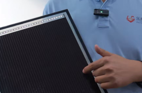
Device Structure: The optimized stack consisted of Mo back contact / a-Si:H p-i-n layers / ZnO:Al (AZO) front contact deposited sequentially on the polyimide substrate, with multiple cells monolithically integrated to form 6×5 cm² modules.
Table: Optimized PECVD Parameters for a-Si:H Deposition
Parameter | Optimal Range | Impact on Film Properties |
|---|---|---|
Deposition Temperature | 190°C | Determines film density and defect states |
Hydrogen Dilution Ratio (R) | 2-40 | Controls stress state and microstructure |
Deposition Rate | 0.1-0.5 nm/s | Affects void density and electronic quality |
RF Frequency | 13.56 MHz | Influences plasma density and film uniformity |
3 Exceptional Performance Under Indoor Conditions
3.1 Efficiency Breakthrough at Low Light Intensity
The optimized flexible modules demonstrated remarkable performance under indoor lighting conditions representative of typical office environments. Under F12 fluorescent spectrum illumination at 300 lux:
Record Efficiency: The modules achieved 9.1% aperture efficiency and 8.7% total area efficiency, representing a significant improvement over previous results (approximately 6%).
Stable Performance Across Illuminance Levels: The modules maintained consistent efficiency across a wide illuminance range from 100 to 5000 lux, indicating absence of significant low-light losses.
Mechanical Robustness: The devices withstood bending radii as small as 2 cm through over 800 bending cycles without significant performance degradation, far exceeding industry standards (typically 5 cm bending radius).
3.2 Reliability and Long-Term Stability
Accelerated aging tests confirmed the exceptional stability of the flexible modules under continuous indoor operation:
Light-Induced Degradation: The optimized hydrogen dilution ratio effectively suppressed the Staebler-Wronski effect (light-induced degradation characteristic of a-Si:H). After 1000 hours of exposure to high-intensity illumination (3000 lux, F12 spectrum including UV component), the modules exhibited less than 10% power degradation.
Thermal Stability: The low-temperature deposition process and polyimide substrate compatibility ensured stable performance across typical indoor temperature variations.
Table: Performance Characteristics of Flexible a-Si:H Modules Under Indoor Conditions
Parameter | Performance Value | Test Conditions |
|---|---|---|
Aperture Efficiency | 9.1% | 300 lux, F12 spectrum |
Total Area Efficiency | 8.7% | 300 lux, F12 spectrum |
Bending Endurance | >800 cycles | 2 cm radius |
Light Stability | <10% degradation | 1000 hours at 3000 lux |
Operating Illuminance Range | 100-5000 lux | Various artificial light sources |
4 Comparative Analysis with Other IPV Technologies
When evaluated against alternative indoor photovoltaic technologies, the flexible a-Si:H modules demonstrate distinct advantages:
Advantages Over Crystalline Silicon: a-Si:H exhibits better spectral matching with indoor light sources (typically strong in visible spectrum) compared to crystalline silicon, which is optimized for broadband solar spectrum.
Superior Stability vs. Emerging Technologies: While perovskite and organic photovoltaics have achieved higher laboratory efficiencies (up to 40% under indoor lighting), they face significant challenges regarding long-term stability and encapsulation requirements.
Manufacturing Maturity: a-Si:H technology benefits from established manufacturing processes and proven scalability, unlike emerging IPV technologies that remain primarily at laboratory scale.
5 Applications in IoT and Wireless Sensor Networks
The combination of flexibility, light weight, and efficient low-light operation makes these modules ideally suited for various autonomous electronic applications:
Wireless Sensor Networks: Direct integration of flexible solar modules onto sensor housings or structural elements enables perpetual operation without battery replacement needs.
Wearable Electronics: The mechanical flexibility allows conformal integration into clothing, smart watches, and medical monitoring devices.
Building-Integrated Applications: Transparent and semi-transparent variants can be incorporated into windows, displays, and architectural elements while generating power from indoor lighting.
6 Future Development Directions
Further improvements in flexible a-Si:H IPV technology are anticipated through several promising research avenues:
Advanced Light Management: Integration of nanostructured interfaces and light-scattering layers could enhance photon capture efficiency without increasing thickness.
Hybrid Tandem Architectures: Combination of a-Si:H with other photovoltaic materials (e.g., perovskite top cells) could optimize spectral utilization while maintaining flexibility.
Improved Manufacturing Economics: Development of high-speed roll-to-roll deposition processes will reduce production costs and enable broader adoption.
Conclusion
The development of efficient flexible a-Si:H thin-film solar modules on polyimide substrates represents a significant milestone in indoor energy harvesting technology. Through optimized PECVD processes, careful interface engineering, and strategic material selection, these modules achieve exceptional performance under indoor lighting conditions while maintaining mechanical robustness necessary for integration into IoT devices and wireless sensor networks. As the demand for autonomous electronic systems continues to grow, such advanced energy harvesting solutions will play an increasingly critical role in enabling sustainable, maintenance-free operation across numerous applications.
Keywords:
Flexible indoor photovoltaics
a-Si:H solar cells IoT
Polyimide substrate solar modules
Indoor light energy harvesting
PECVD optimization thin-film silicon
Low-light photovoltaic efficiency
Mechanical flexibility solar cells
Wireless sensor network power
Amorphous silicon indoor performance
Roll-to-roll manufacturing photovoltaics

