Thermal Management in Laser Processing: Lecheng’s Green Picosecond Lasers Limit Heat Damage to <1μm
1. The Critical Challenge of Heat Accumulation in Precision Laser Applications
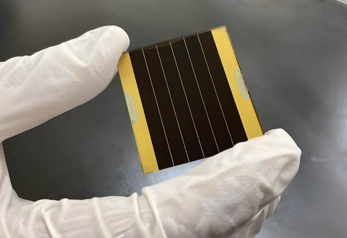
In high-precision manufacturing processes such as perovskite solar cell scribing, flexible circuit board (FPC) drilling, and medical device fabrication, uncontrolled heat propagation remains a major technical bottleneck. Conventional laser systems using nanosecond or continuous-wave lasers often generate heat-affected zones (HAZ) exceeding 10μm, causing material degradation, delamination, and functional failures. For temperature-sensitive materials like perovskite films, organic layers in OLED displays, or thin metal coatings, even minor thermal damage can compromise product performance and yield. Lecheng Intelligent addresses this fundamental challenge through advanced green picosecond laser technology, which delivers ultra-short pulses (10⁻¹² seconds) at 532nm wavelength—a spectrum optimally absorbed by most industrial materials without excessive thermal diffusion. By controlling pulse duration below the material’s thermal relaxation time, Lecheng’s systems localize energy deposition to a microscopic volume, reducing HAZ to less than 1μm. This breakthrough is particularly vital for P2/P3 scribing in perovskite cells, where heat-induced defects near TCO layers can significantly reduce cell efficiency and longevity.
2. Lecheng’s Technological Innovation: How Green Picosecond Lasers Achieve Sub-Micron Thermal Control
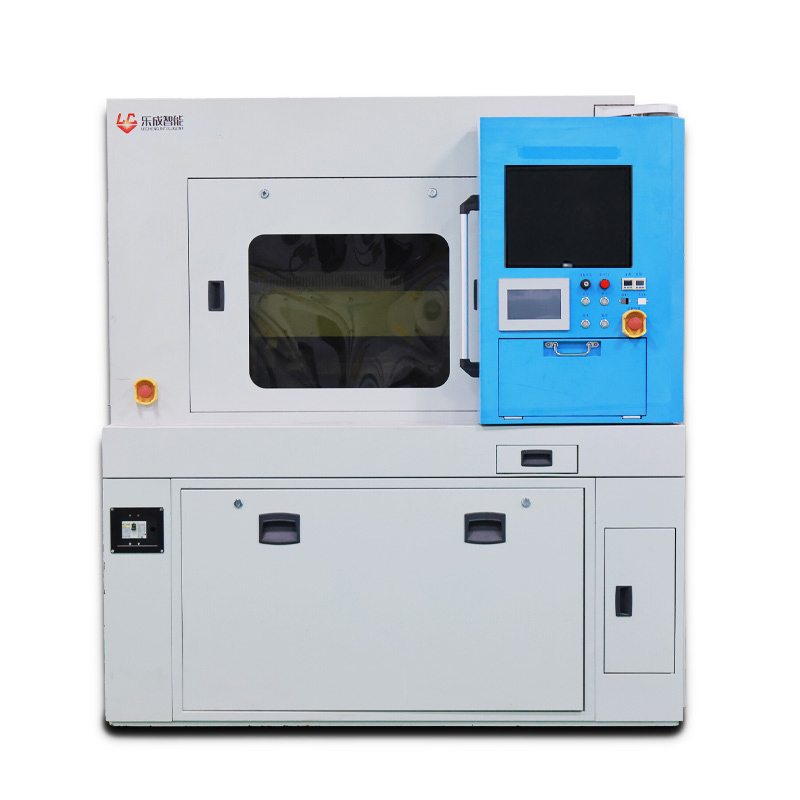
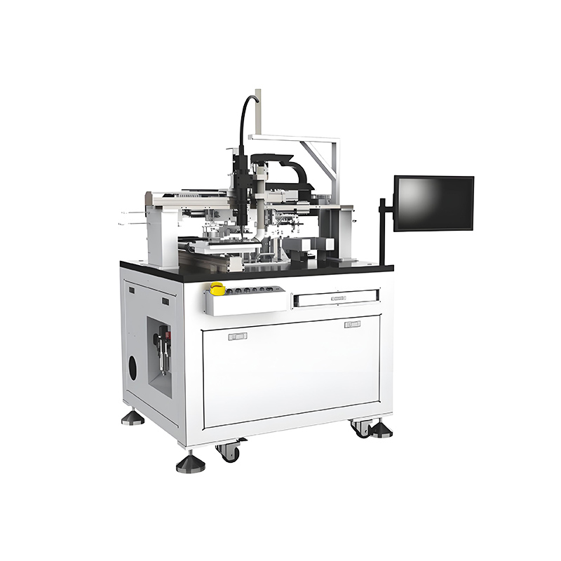
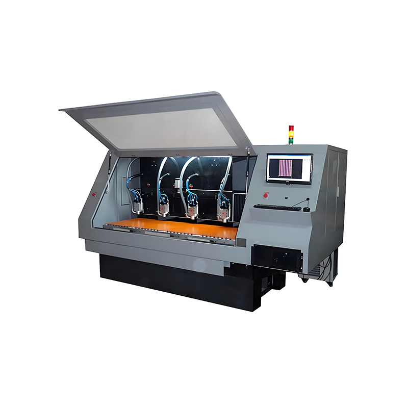
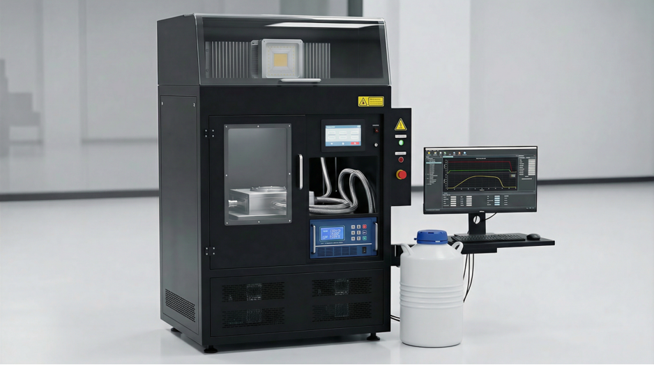
Lecheng’s green picosecond laser systems integrate three core innovations to achieve unprecedented thermal management. First, the proprietary beam-shaping optics homogenize energy distribution across the laser spot, eliminating hot spots that cause localized overheating. Second, adaptive pulse-train modulation allows real-time adjustment of pulse repetition rates (1kHz-2MHz) and duty cycles based on material thickness and thermal conductivity—critical when processing multilayer stacks like perovskite structures (TCO/HTL/Perovskite/ETL). Third, the company’s closed-loop cooling system maintains laser head temperature within ±0.1°C, ensuring consistent beam quality during extended operations. In practical applications, these technologies enable Lecheng’s lasers to achieve remarkable results: P2 scribing on perovskite cells with HAZ below 1μm while maintaining scribe widths of 30-60μm; drilling 50μm micro-vias in FPCs without carbonization; and cutting 0.3mm tungsten sheets with edge integrity surpassing medical standards. Compared to infrared lasers, the 532nm green wavelength reduces photon energy requirements by 30% for equivalent ablation thresholds, minimizing collateral thermal effects in heat-sensitive applications.
3. Industry Applications: From Renewable Energy to Medical Devices
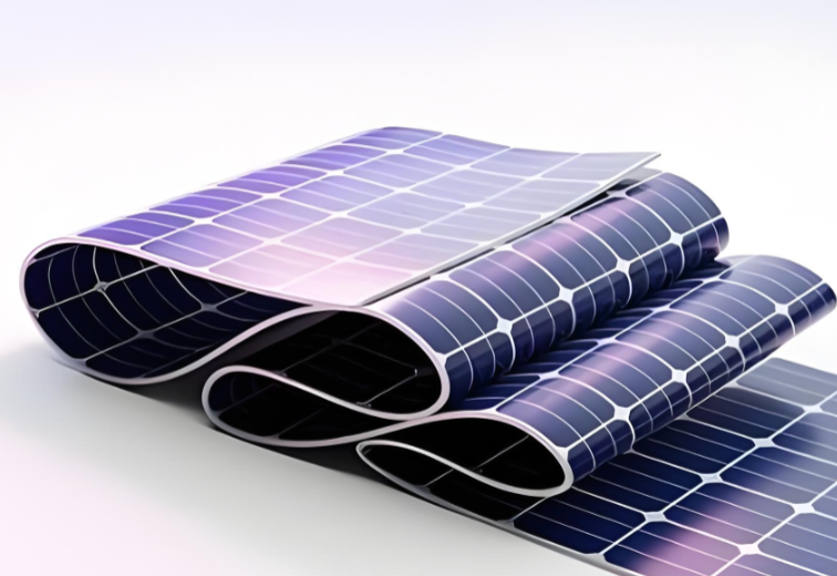
The sub-micron thermal management capability of Lecheng’s green picosecond lasers unlocks new possibilities across high-tech industries. In perovskite solar manufacturing, HAZ control below 1μm prevents TCO layer degradation during P2/P3 scribing, increasing module conversion efficiency by 3-5% and extending operational lifetime. For flexible electronics, the technology enables precise patterning of copper/polyimide layers without warping or adhesion loss—critical for foldable displays and wearable sensors. In medical device production, lasers process bio-compatible materials (e.g., titanium implants, polymer catheters) with surgical precision while avoiding thermal alteration of material properties. Lecheng’s systems also support emerging applications such as glass-internal marking for automotive glass (HAZ <5μm) and silicon wafer dicing for semiconductors. Through partnerships with industry leaders, Lecheng continuously optimizes laser parameters for specific materials—from transparent conductive oxides to shape-memory alloys—demonstrating versatility in solving thermal challenges across manufacturing sectors.
Conclusion
Lecheng Intelligent’s green picosecond laser technology sets a new benchmark in thermal management for precision manufacturing. By confining heat damage to sub-micron scales, it enables higher yields, finer features, and new material applications—accelerating innovation in sustainable energy, electronics, and healthcare.

