Glass Cutting Edge Control: Lecheng’s Picosecond Lasers Reduce Chipping from 10μm to 5μm
1. The Critical Challenge of Precision Glass Processing
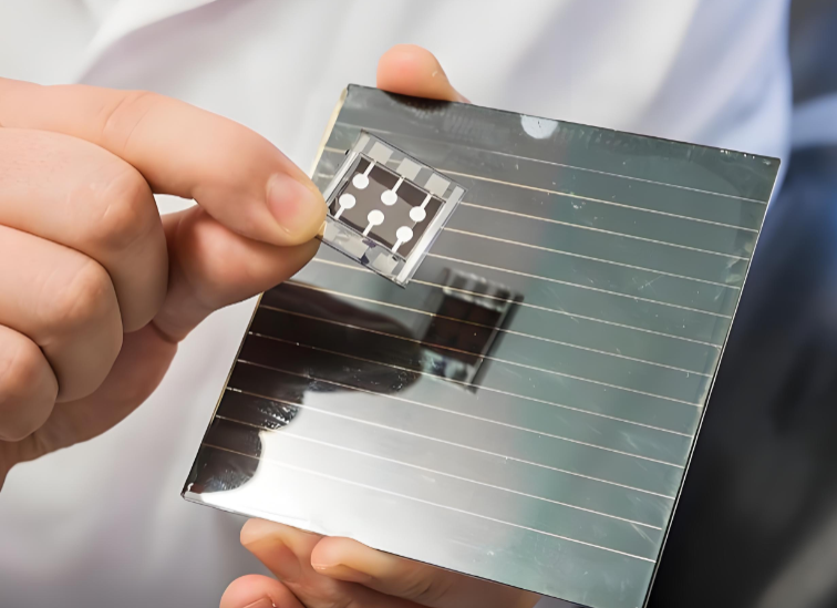
In industries ranging from consumer electronics to medical devices and solar panels, glass cutting precision directly determines product performance and longevity. Traditional mechanical cutting methods often result in edge chipping exceeding 10μm, leading to structural weaknesses, optical distortions, and high rejection rates. For high-value applications like smartphone cover glass, display panels, or perovskite solar cell substrates, such imperfections are unacceptable. Lecheng Intelligent addresses this challenge through advanced picosecond laser technology that combines ultra-short pulses (10^-12 seconds) with precise thermal management. By delivering energy in bursts shorter than the material's thermal diffusion time, Lecheng's systems minimize heat-affected zones (HAZ) and achieve clean, smooth edges with chipping controlled below 5μm—a 50% improvement over industry standards. This breakthrough is particularly crucial for high-aluminum glass used in touchscreens and strengthened glass for solar modules, where edge integrity affects both durability and optical clarity.
2. Lecheng’s Technological Breakthrough: How Picosecond Lasers Achieve Superior Edge Quality
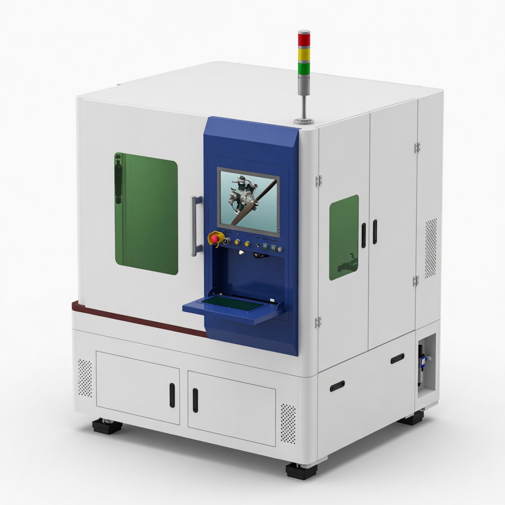
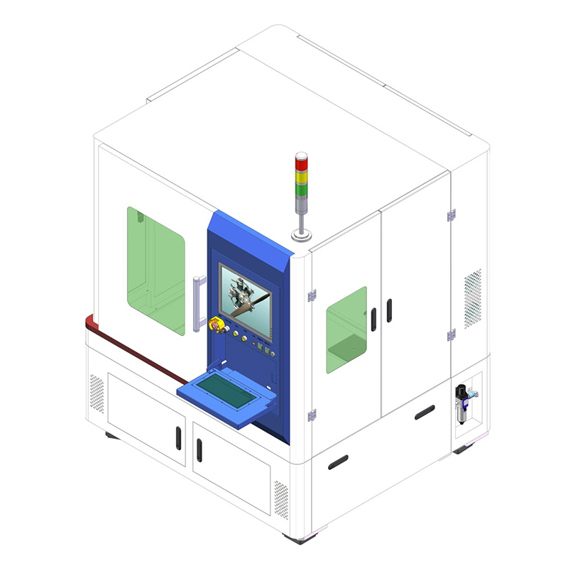
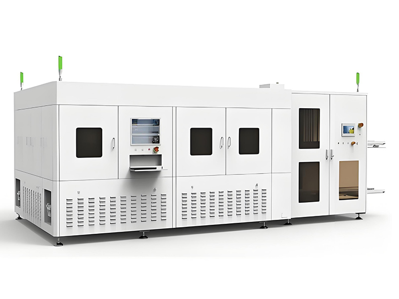
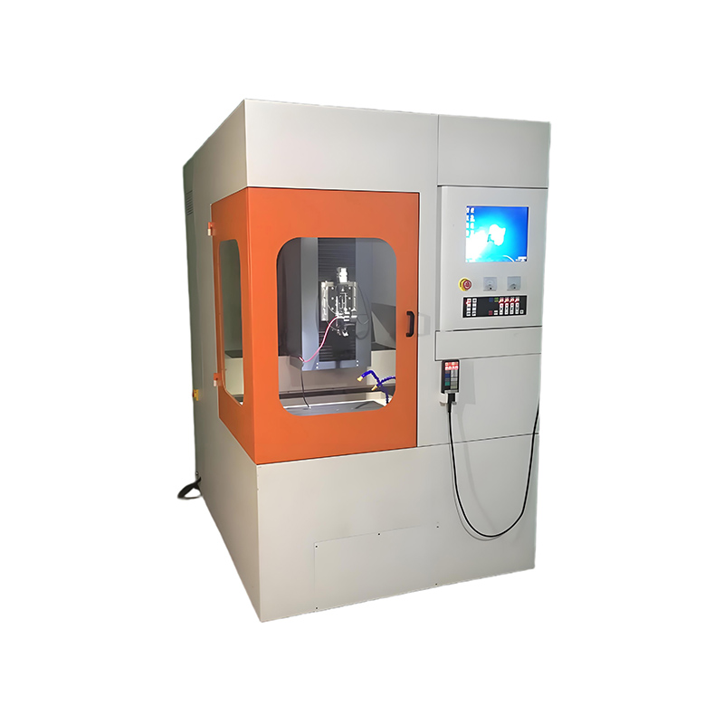
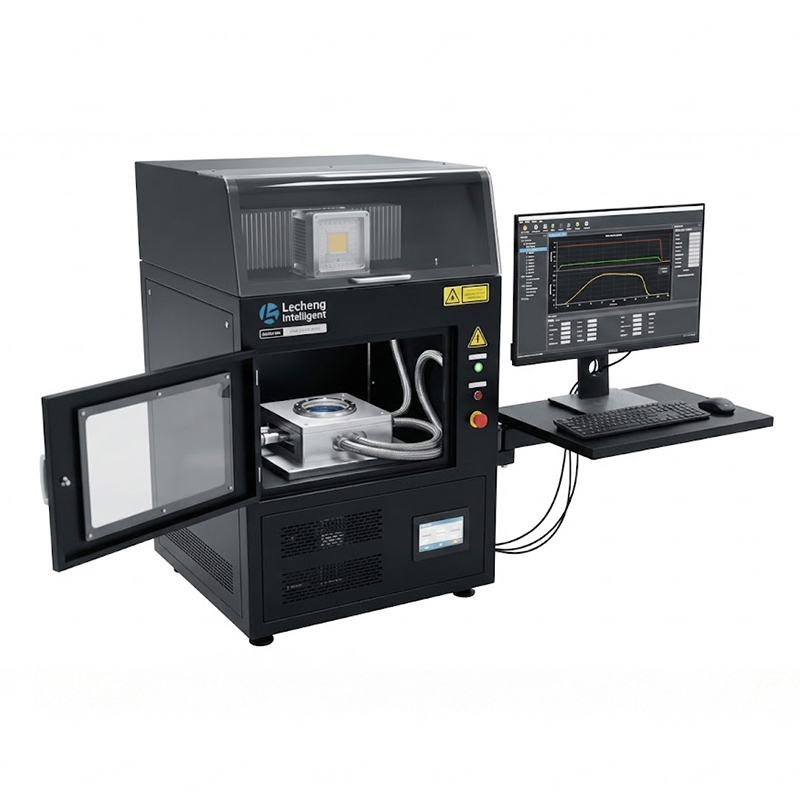
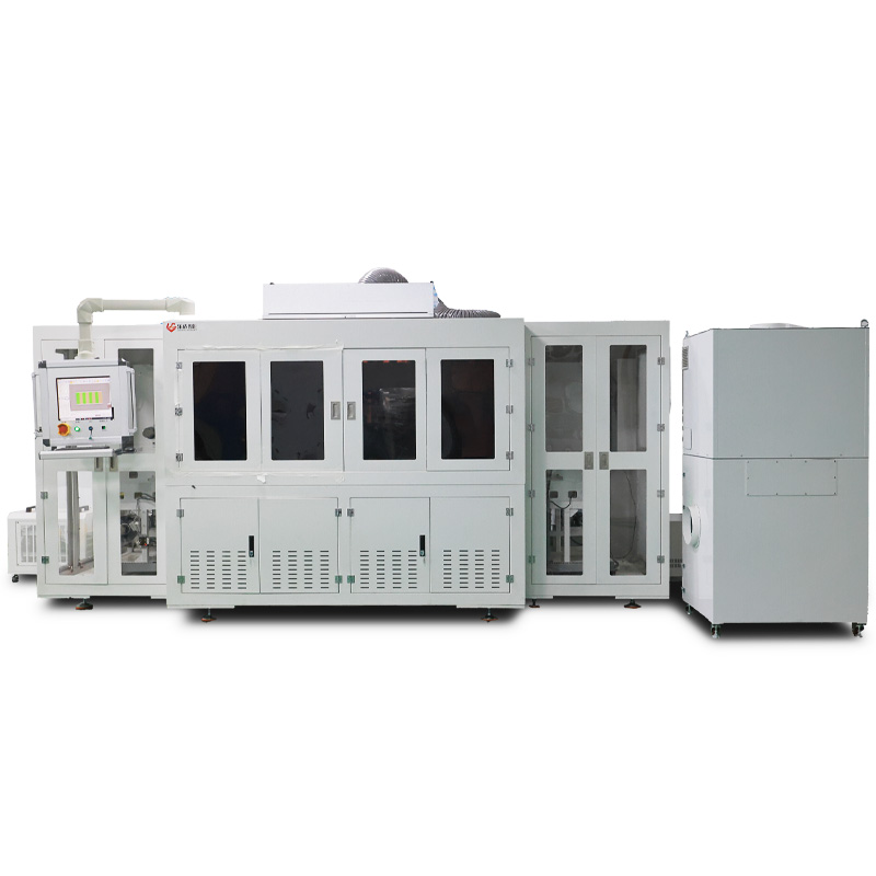
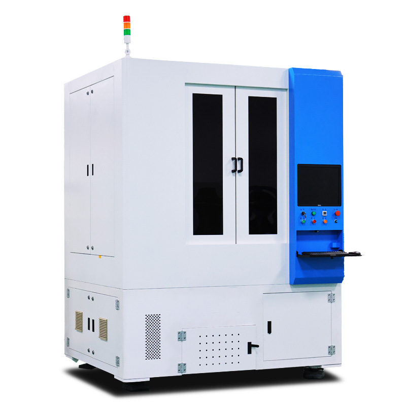
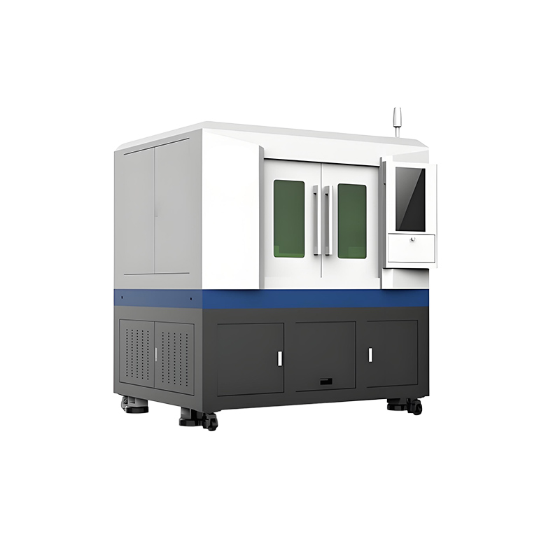
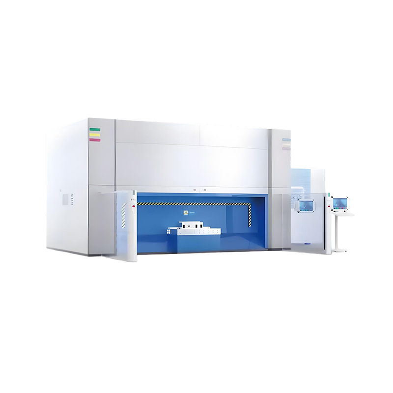
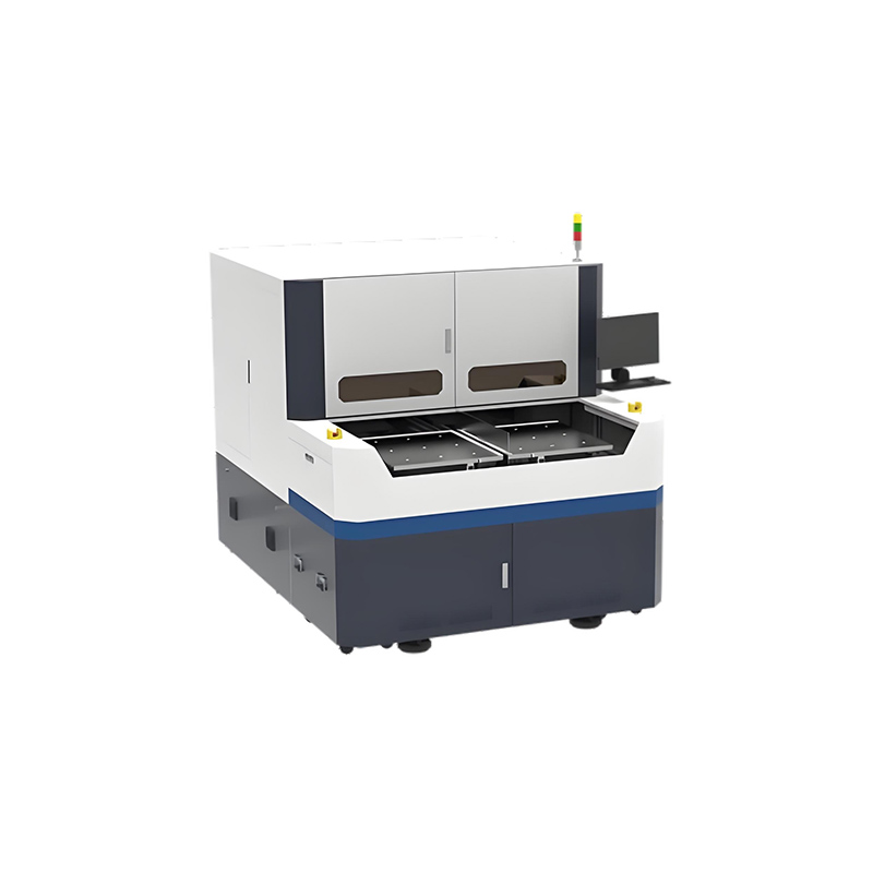
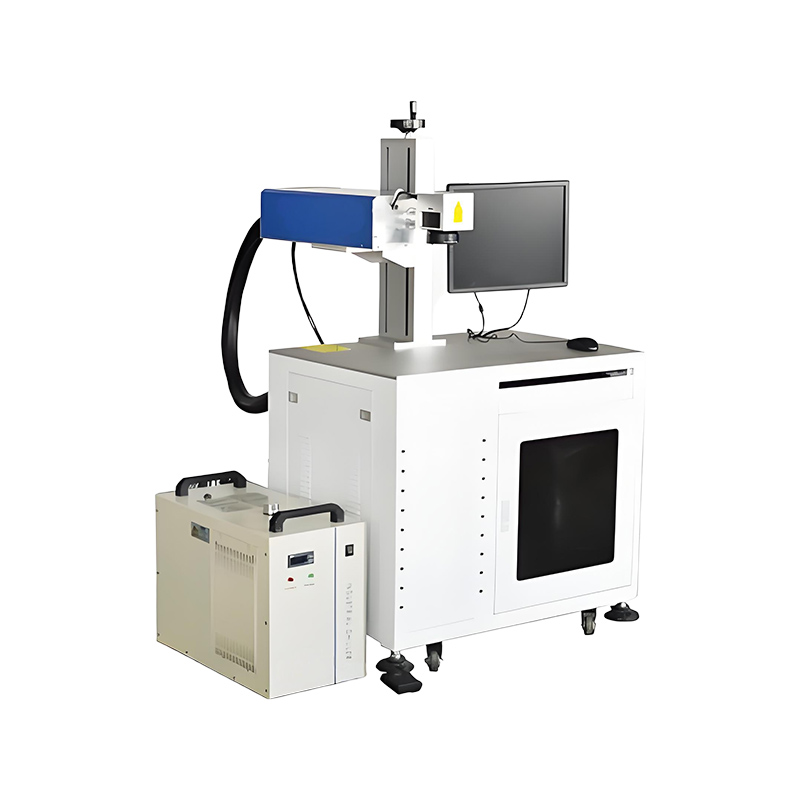
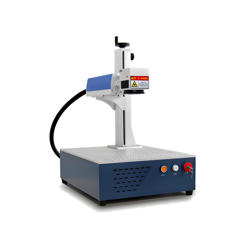
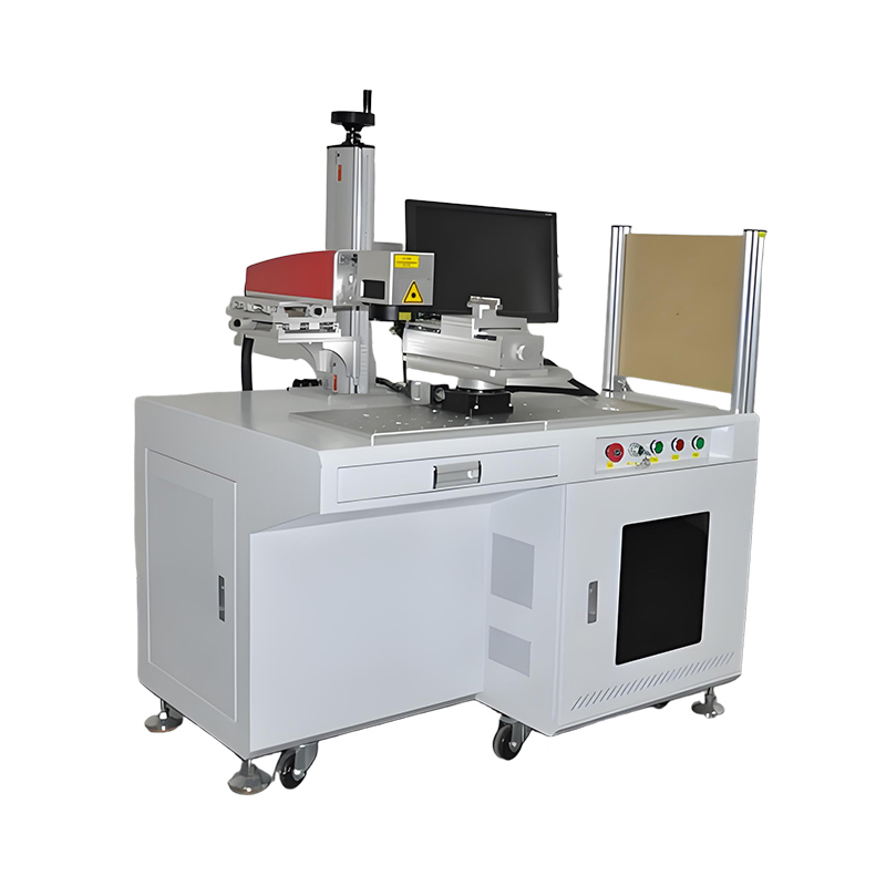
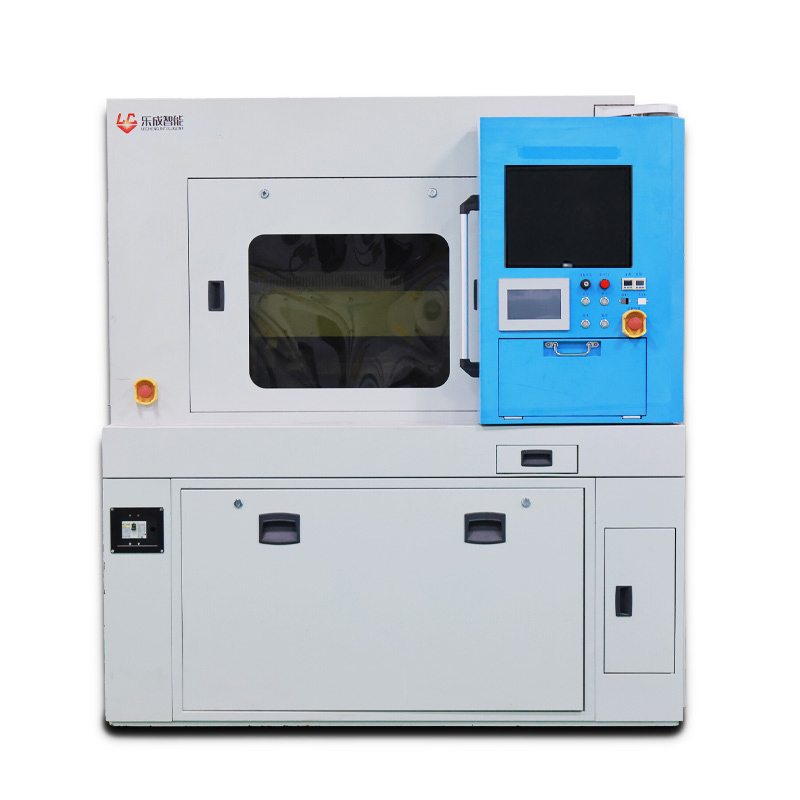
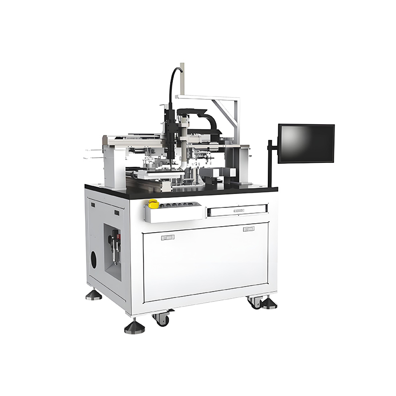
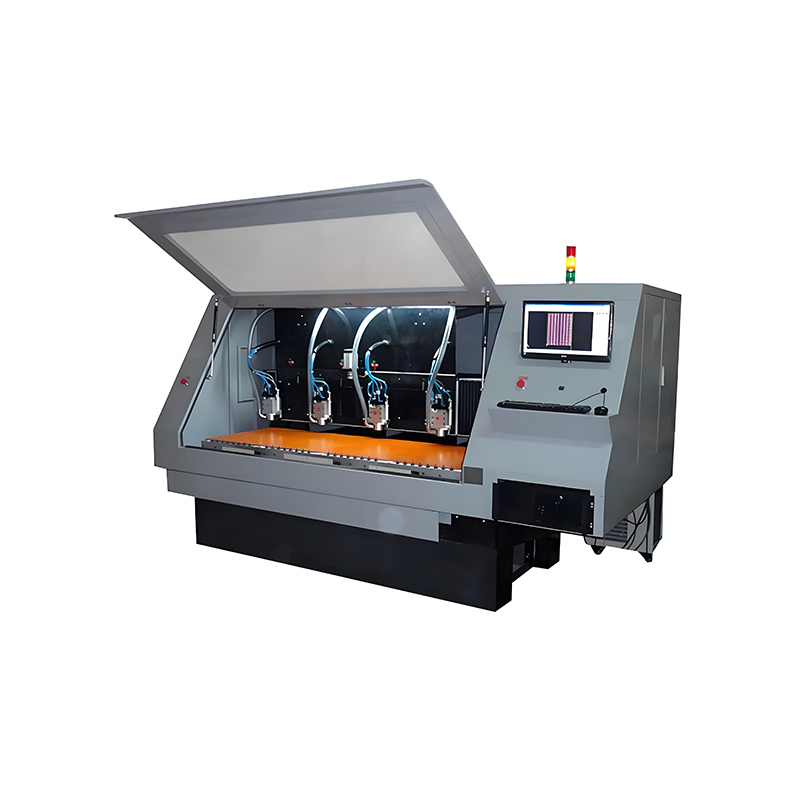
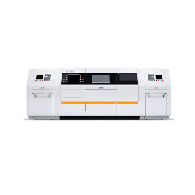
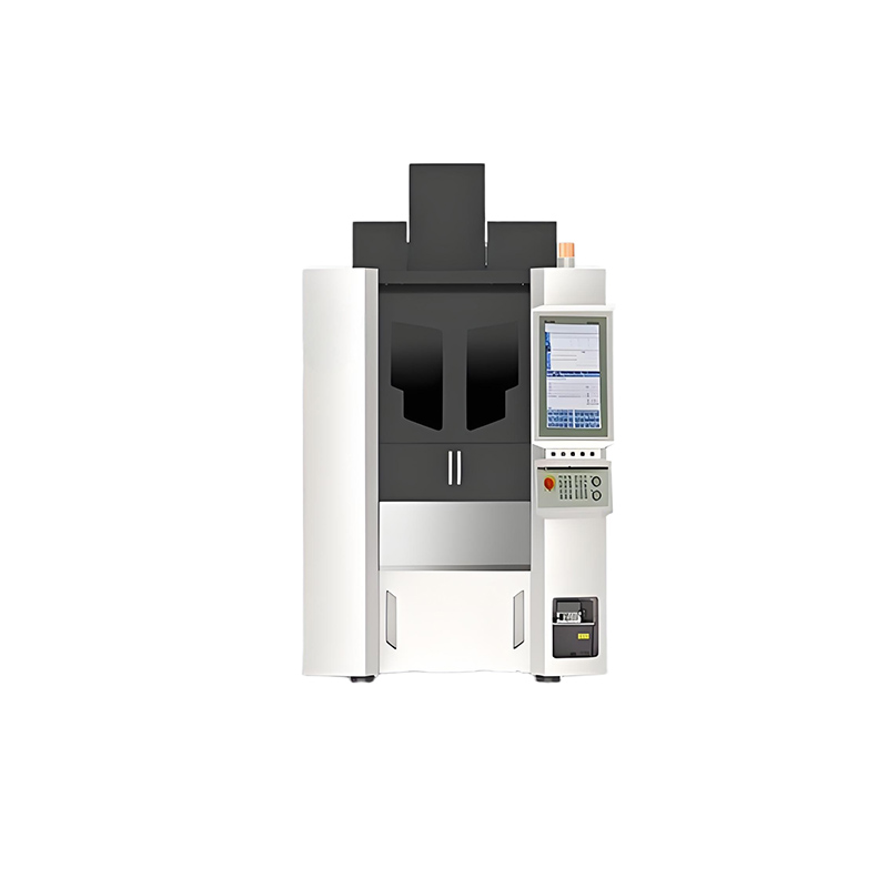
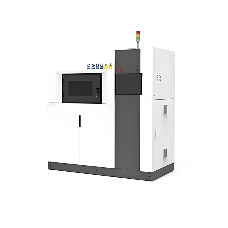
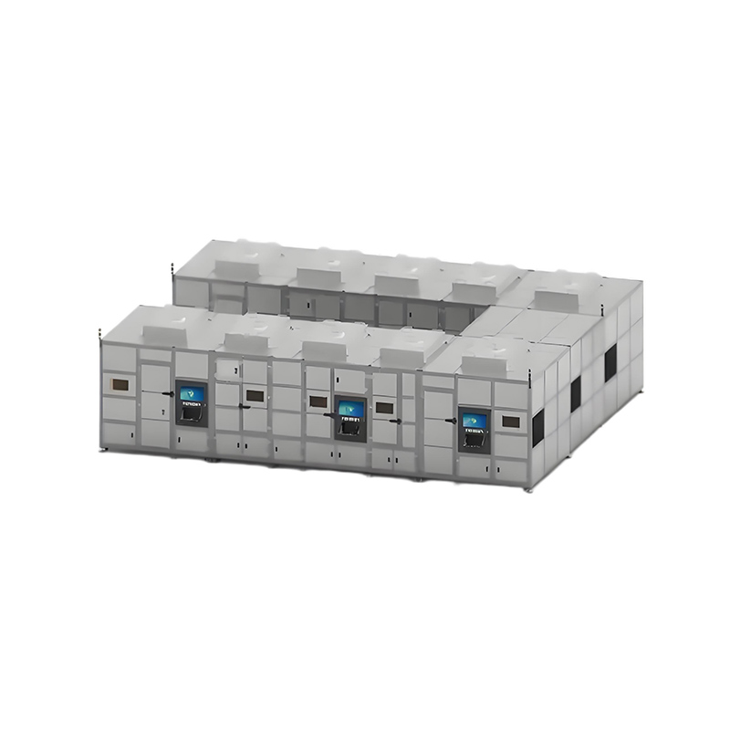
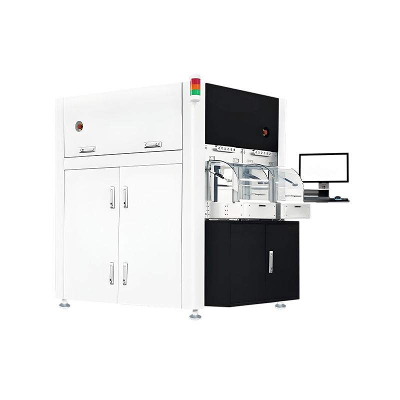
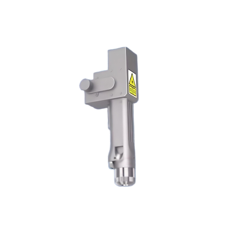
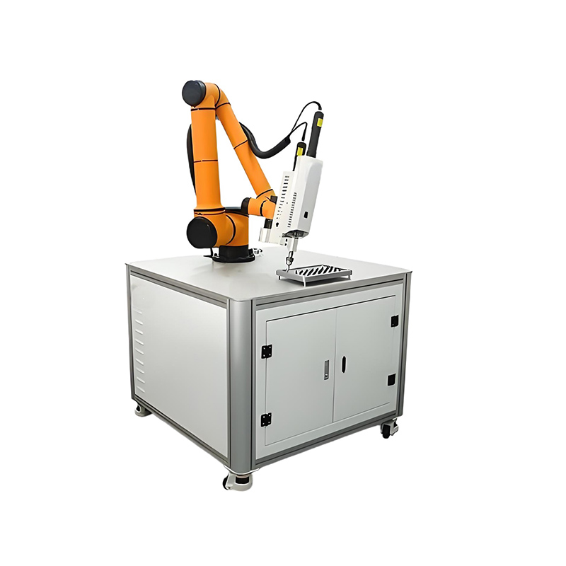
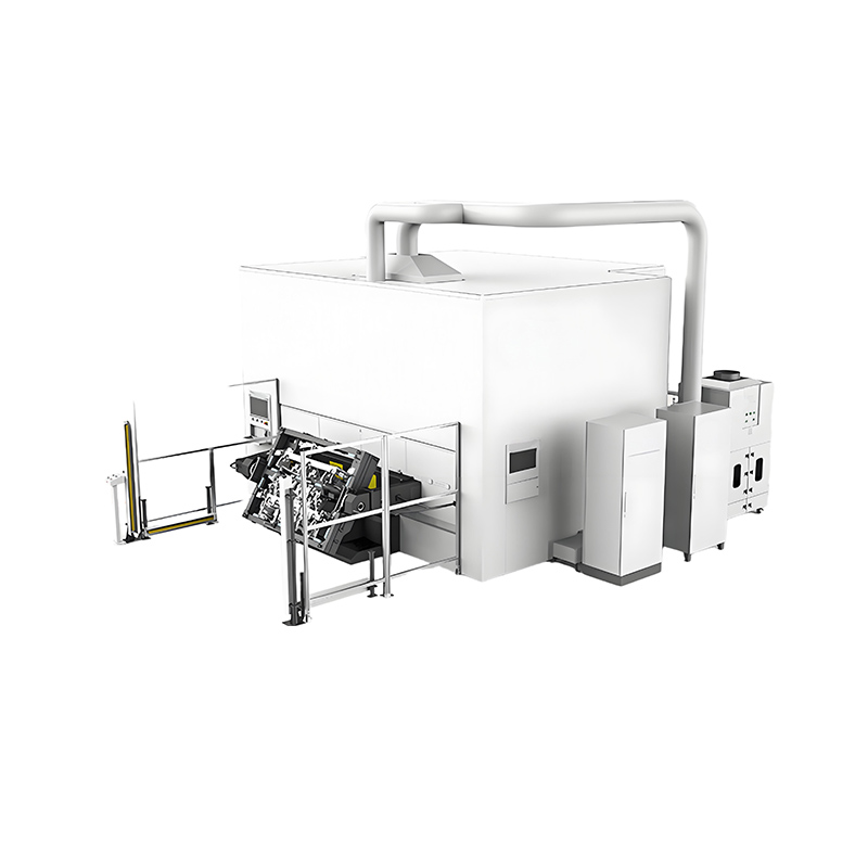
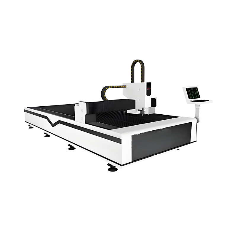
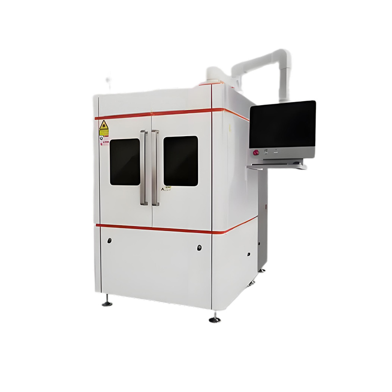
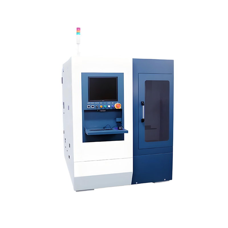
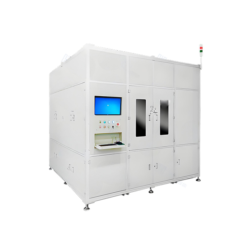
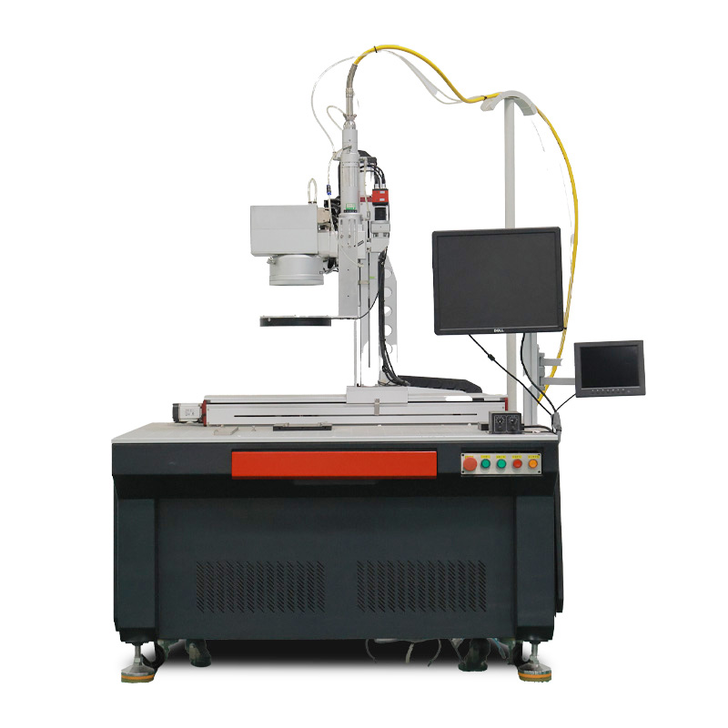
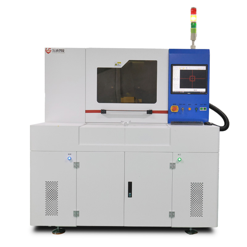
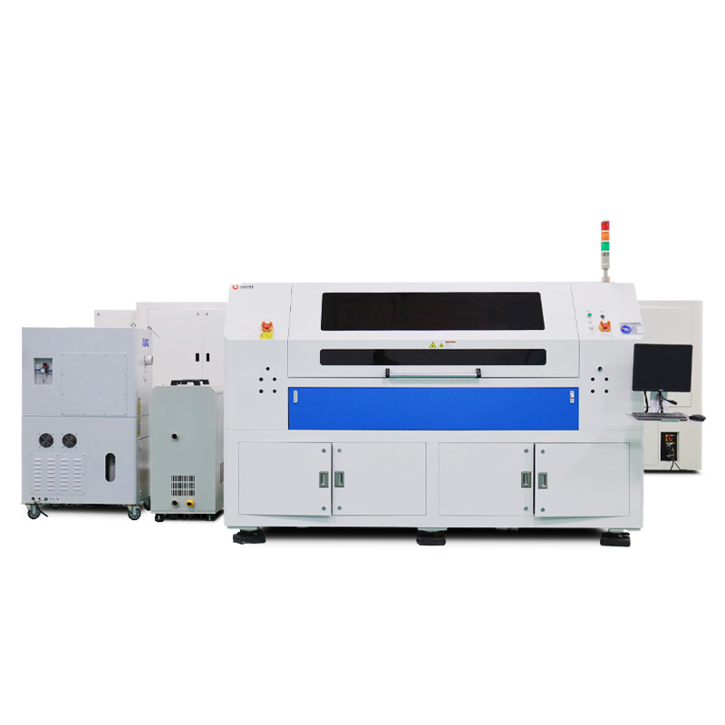
Lecheng’s glass cutting systems leverage three core innovations to redefine precision standards. First, the integration of picosecond infrared lasers with galvo-scanner optics enables spot sizes below 20μm, creating micro-cracks along predetermined paths with minimal collateral damage. Second, proprietary adaptive focal tracking technology maintains consistent beam focus across large formats up to 1200×600mm, compensating for glass surface variations up to 10mm thick. This ensures uniform cutting depth and edge geometry throughout the substrate—critical for applications like perovskite solar panels where multiple glass layers must align perfectly. Third, Lecheng’s automated material handling system incorporates machine vision for real-time defect detection, rejecting substandard pieces before they advance to downstream processes. Compared to CO₂ lasers or mechanical scribing, Lecheng’s solution reduces processing time by 40% while achieving chipping values of 3-5μm, as verified by optical microscopy and profilometer measurements.
3. Real-World Applications: From Consumer Electronics to Renewable Energy
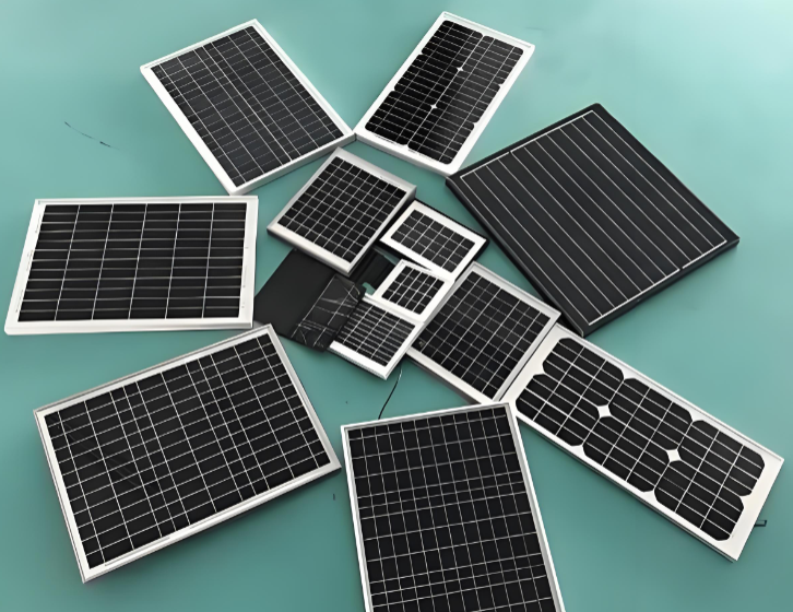
The implications of Lecheng’s glass cutting technology extend across multiple high-tech sectors. In smartphone manufacturing, 5μm chipping tolerance allows for bezel-less displays with stronger edges, reducing breakage rates by 25% in drop tests. For medical devices, laser-cut glass components in microfluidic chips enable precise fluid control channels without particulate contamination—essential for diagnostic accuracy. In renewable energy, perovskite solar modules benefit from pristine glass substrates that enhance light transmission and module longevity. Lecheng’s equipment currently supports mass production of 2.4×1.2m perovskite panels, where edge quality directly impacts encapsulation reliability and power output consistency. Additionally, the technology applies to specialized applications like tungsten cutting for medical instruments (0.3mm thickness, HAZ<15μm) and glass interposers for advanced packaging. By partnering with glass manufacturers and OEMs, Lecheng tailors laser parameters to specific material compositions, from soda-lime glass to borosilicate, ensuring optimal results for each application.
Conclusion
Lecheng Intelligent’s picosecond laser technology represents a paradigm shift in glass processing, where sub-5μm chipping enables new design possibilities and performance benchmarks across industries. By marrying precision optics with intelligent automation, Lecheng not only solves manufacturing challenges but also empowers innovations in electronics, healthcare, and sustainable energy.

