Perovskite Thin Film Preparation Methods
The preparation of perovskite materials is a critical step in achieving high-efficiency perovskite solar cells. At the molecular scale, PbI₂ and CH₃NH₃I can rapidly react through self-assembly to form CH₃NH₃PbI₃. Thus, whether in solid, liquid, or gas phases, thorough mixing of the two raw materials can yield the desired perovskite material. However, for thin-film solar cell light-absorbing layers with thicknesses below 1 μm, the large perovskite crystals produced by solid-phase reaction methods are clearly unsuitable.

The earliest method for preparing perovskite thin films for solar cells was the one-step liquid-phase method, where stoichiometric ratios of PbI₂ and CH₃NH₃I are dissolved in solvents such as γ-butyrolactone or N,N-dimethylformamide (DMF). A certain amount of the solution is dropped onto a nanoporous scaffold layer and spin-coated at a specific speed. After heating to remove the solvent, a photoanode filled with perovskite is obtained. For preparing chlorine-doped perovskites, PbCl₂ and an excess of CH₃NH₃I are used as precursors. After solvent removal and heat treatment, the stoichiometric portion of halomethylamine and lead halide forms the perovskite, while the excess portion evaporates.
The two-step liquid-phase method separates the deposition of PbI₂ and the formation of perovskite into two steps: First, a solution of PbI₂ at a certain concentration is spin-coated onto the porous scaffold layer. The PbI₂-coated film is then immersed in a solution of methylammonium iodide in isopropanol, gradually converting the yellow PbI₂ into dark brown perovskite.
H. Snaith et al. developed a vapor co-evaporation deposition method for preparing perovskite thin films. This technique also enables high-efficiency perovskite solar cells but requires complex co-evaporation equipment for lead halide and methylammonium halide. Additionally, vapor-assisted liquid-phase methods have recently emerged as a new technology. This approach involves spin-coating a PbI₂ film and then exposing it to CH₃NH₃I vapor, allowing slow perovskite formation. Compared to co-evaporation methods, this vapor-assisted liquid-phase technique reduces experimental equipment requirements.
All the aforementioned perovskite thin film preparation methods can achieve efficiencies exceeding 12%. However, the spin-coating process used in liquid-phase methods is difficult to scale for mass production.
Expanded into a Technological Article (Approx. 1200 words):
Advancements in Perovskite Thin Film Fabrication: Techniques and Challenges Towards Scalability
Introduction
Perovskite solar cells (PSCs) have witnessed an unprecedented rise in power conversion efficiency (PCE), from 3.8% in 2009 to over 26% in recent years for small-area devices. However, translating these efficiencies to large-area modules remains a significant challenge. The core of this challenge lies in the preparation of high-quality, uniform perovskite thin films. The fabrication method not only determines the optoelectronic properties but also impacts the scalability and commercial viability of perovskite solar technology.
1. Fundamental Fabrication Techniques
1.1 One-Step Liquid-Phase Method
This method involves dissolving stoichiometric amounts of PbI₂ and CH₃NH₃I in polar solvents like DMF or γ-butyrolactone. The solution is deposited onto a substrate via spin-coating, and thermal annealing removes the solvent, forming the perovskite layer. For chlorine-doped variants (e.g., CH₃NH₃PbI₃₋ₓClₓ), PbCl₂ and excess CH₃NH₃I are used. The excess organic component evaporates during annealing. While simple, this method struggles with controlling crystallization kinetics, often leading to pinholed and inhomogeneous films on larger substrates.
1.2 Two-Step Liquid-Phase Method
Here, PbI₂ is first deposited onto the substrate. Subsequently, the film is immersed in a solution of CH₃NH₃I in isopropanol, converting PbI₂ to perovskite. This sequential approach offers better control over the conversion process and often yields more uniform films. However, incomplete conversion and residual PbI₂ can act as charge recombination centers, limiting device performance.
1.3 Vapor-Phase Deposition Methods
To overcome the limitations of solution processing, vapor-based techniques have been developed.
Vapor Co-Evaporation: Developed by groups like Snaith's, this requires simultaneous thermal evaporation of PbI₂ and CH₃NH₃I in a high-vacuum chamber. It produces high-quality, pinhole-free films with precise compositional control but involves expensive equipment and low throughput.
Vapor-Assisted Solution Process (VASP): A hybrid approach where a solution-processed PbI₂ film is exposed to CH₃NH₃I vapor. The vapor diffuses into the solid film, converting it to perovskite. This method reduces the need for complex vacuum systems and often results in films with superior crystallinity and coverage compared to purely solution-based methods.
2. Overcoming Scalability Challenges
The transition from lab-scale spin-coating to industry-compatible methods is crucial for commercialization.
2.1 Scalable Coating Techniques
Research is focused on techniques like:
Blade Coating: A meniscus-guided coating method where a blade spreads the precursor ink over a substrate. It offers high material utilization and is compatible with roll-to-roll (R2R) processing. Key challenges include controlling fluid dynamics and crystallization during the fast drying process.
Slot-Die Coating: Another R2R-compatible technique that pre-meteres the ink, enabling precise control over film thickness and uniformity. Efficient solvent removal strategies, like nitrogen quenching, are often integrated to manage crystallization.
Spray Coating: Suitable for large and irregular surfaces, but achieving uniform, pinhole-free films remains difficult.
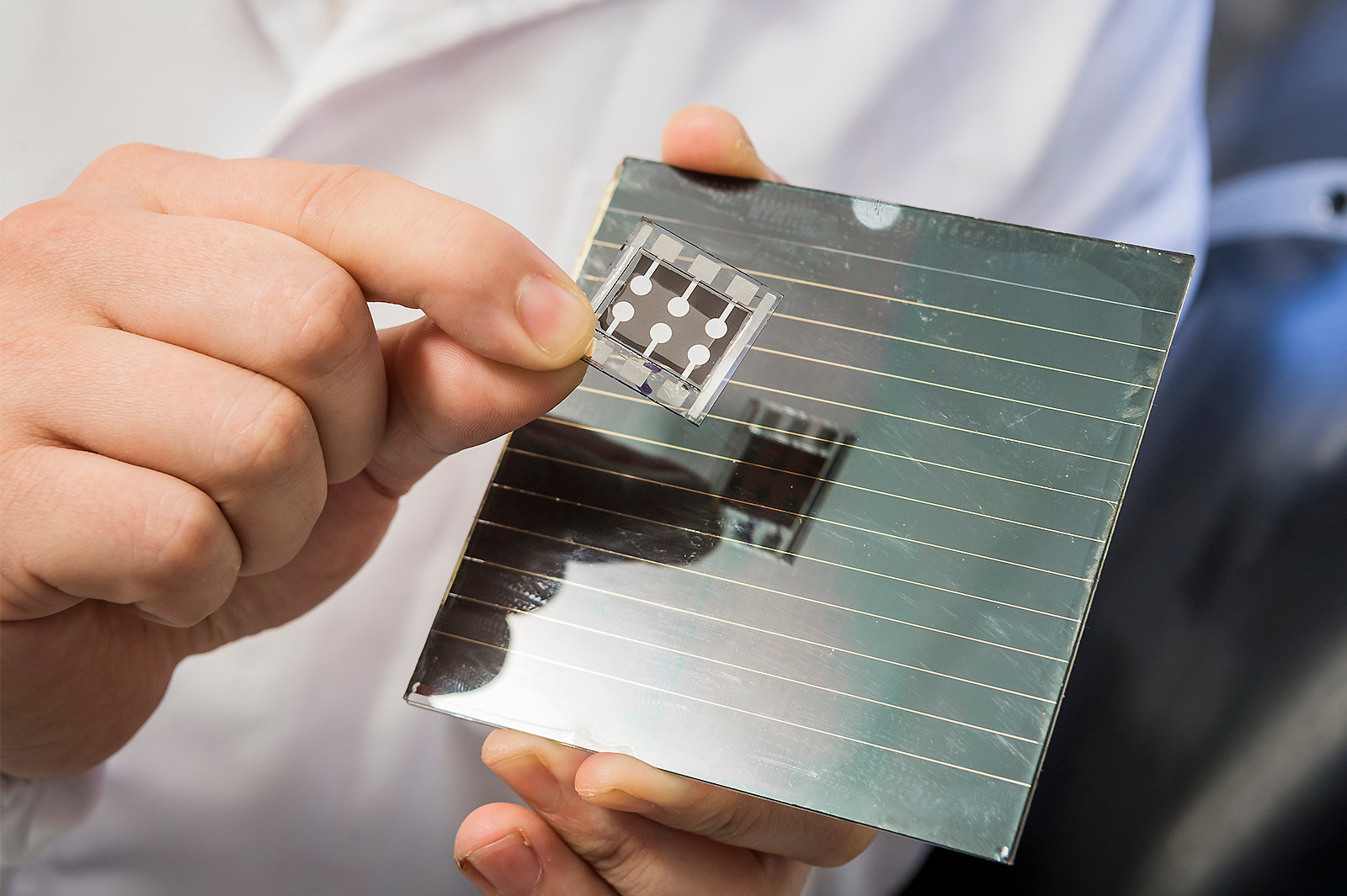
2.2 Crystallization Engineering
Controlling the crystallization process is vital for obtaining high-quality films over large areas. Strategies include:
Additive Engineering: Incorporating additives like MACl or DMSO into the precursor ink can modulate crystallization kinetics, leading to larger grains and reduced defect density.
Gas Quenching: Using blown gas (e.g., air, N₂) during or after deposition accelerates solvent evaporation, promoting rapid and uniform nucleation.
Vacuum Flash-Assisted Methods: Applying a vacuum after solution deposition rapidly evaporates the solvent, leading to the formation of dense intermediate phases that can be converted to high-quality perovskite upon annealing.
2.3 Compositional Engineering
Exploring lead-reduced and stable perovskite compositions is essential for sustainability and stability. Partial substitution of Pb with Sn or formamidinium (FA⁺) for methylammonium (MA⁺) can tune the bandgap and improve thermal stability.
3. Industrial Outlook and Challenges
While techniques like blade coating and slot-die coating have demonstrated PCEs over 20% on small areas, their performance on large-area modules still lags. Key challenges include:
Film Uniformity: Maintaining thickness and compositional homogeneity over meters is non-trivial. Inhomogeneities lead to current losses and reduced fill factors.
Defect Management: Scalable deposition often introduces more defects, necessitating the development of scalable passivation strategies.
Throughput and Cost: Balancing processing speed with film quality is critical for reducing manufacturing costs.
Stability: Achieving long-term operational stability under real-world conditions (heat, humidity, light, bias) for large-area modules is the ultimate hurdle before widespread adoption.
Promisingly, companies and research institutes are piloting large-area perovskite module production. For instance, fully printed mini-modules using R2R techniques have achieved efficiencies around 11% on active areas of ~50 cm².
Conclusion
The journey of perovskite thin film fabrication has evolved from simple spin-coating to sophisticated vapor-assisted and scalable printing techniques. While challenges in scalability, stability, and efficiency retention for large areas persist, the rapid progress offers strong optimism. Continuous innovation in deposition technology, crystallization control, and material design is paving the way for perovskite solar cells to transition from a lab curiosity to a commercial photovoltaic technology

