Introduction to Perovskite Solar Cells
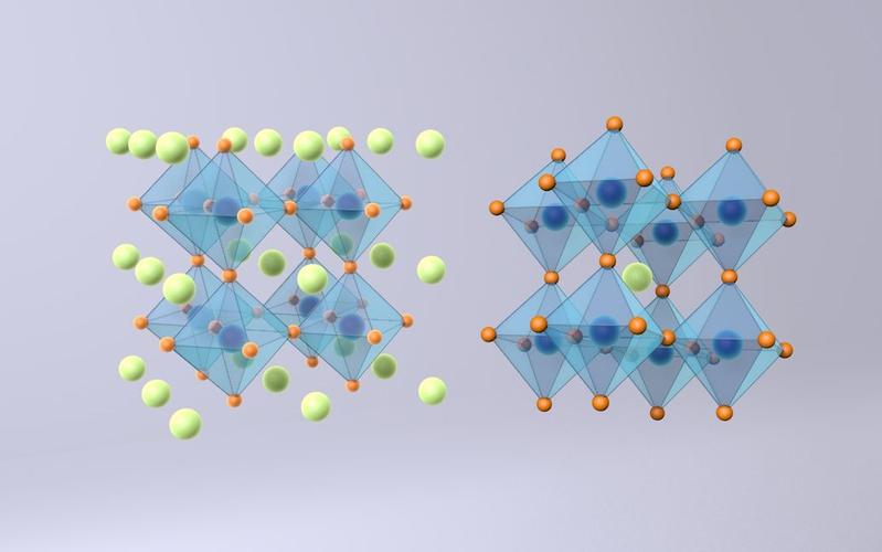
The structure of perovskite solar cells is illustrated in the figure below. Its core is a light-absorbing material composed of organometal halides with a perovskite crystal structure (ABX₃) (unit cell structure shown in the attached figure). In this perovskite ABX₃ structure, A is the methylammonium group (CH₃NH₃⁺), B is a metal lead atom, and X is a halogen atom such as chlorine, bromine, or iodine. Currently, the most common perovskite material in high-efficiency perovskite solar cells is methylammonium lead iodide (CH₃NH₃PbI₃). It has a bandgap of approximately 1.5 eV and a high extinction coefficient; a film just a few hundred nanometers thick can sufficiently absorb sunlight up to 800 nm. Moreover, this material is simple to prepare—a uniform film can be obtained by spin-coating a solution containing PbI₂ and CH₃NH₃I at room temperature. These properties enable the perovskite-type structure CH₃NH₃PbI₃ to not only absorb visible light and part of the near-infrared spectrum but also generate photogenerated carriers that are less prone to recombination, with minimal energy loss. This is the fundamental reason why perovskite solar cells can achieve high efficiency.
Figure: Crystal structure of perovskite material (using CH₃NH₃PbI₃ as an example) and schematic diagram of a perovskite solar cell structure.
Due to the relatively complex crystal structure, which imposes strict requirements on the radii of the atoms (or groups) at the A, B, and X sites, the composition of perovskite light-absorbing materials is relatively fixed. Recently, some research groups have replaced the methylammonium group at the A site with formamidinium (FA⁺), narrowing the bandgap to 1.48 eV and achieving higher photocurrent. For the B site, replacing lead (Pb) with tin (Sn) has not yet resulted in any reported photoelectric response. For the X site, atoms such as chlorine, bromine, or iodine can be used, but only iodine-based perovskites have a suitable bandgap for high conversion efficiency. Besides CH₃NH₃PbI₃, CH₃NH₃PbI₃₋ₓClₓ is also widely studied. While maintaining the basic energy level structure, a small amount of chlorine doping can improve electron mobility, demonstrating superior photoelectric performance. However, compared to silicon-based materials, commonly used perovskite light-absorbing materials have drawbacks such as insufficiently broad light response range, sensitivity to water and some solvents, and containing heavy metal lead. Therefore, finding perovskite materials with narrower bandgaps, better chemical stability, and environmental friendliness is highly meaningful.
The development of perovskite thin-film solar cells originated from dye-sensitized solar cells (DSSCs). Leveraging technologies accumulated over the past two decades in DSSCs, organic solar cells, and others, perovskite solar cells have developed rapidly. The earliest perovskite solar cells used CH₃NH₃PbI₃ to sensitize TiO₂ photoanodes and a liquid I₃⁻/I⁻ electrolyte, achieving an efficiency of only 3.8% (optimized to 6.5%). However, due to the instability of CH₃NH₃PbI₃ in the liquid I₃⁻/I⁻ electrolyte, the cell stability was poor, and research in this area is now limited. Replacing the liquid I₃⁻/I⁻ electrolyte with a solid-state hole transport material (HTM) (e.g., spiro-OMeTAD, P3HT) greatly improved cell efficiency, reaching 16%, surpassing the highest efficiency of dye-sensitized solar cells (13%) and demonstrating good stability.
Building on this, H. Snaith et al. replaced the porous scaffold layer n-type semiconductor TiO₂ with an insulating material such as Al₂O₃ or ZrO₂ and assembled thin-film cells using hole transport materials, also achieving high efficiency (the reported highest efficiency was 15.9%). This result indicates that the perovskite material CH₃NH₃PbI₃ itself has good electron conduction capability. Perovskite solar cells based on insulating material scaffold layers have, in principle, moved beyond the traditional sensitization concept, becoming a mesoscopic superstructured heterojunction solar cell. Furthermore, by removing the insulating scaffold layer and using a uniform high-quality perovskite film, a planar heterojunction cell can also achieve high efficiency (the reported highest efficiency is 15.7%). On the other hand, even without hole transport materials, a heterojunction cell formed between perovskite and porous TiO₂ has reached an efficiency of 10.5%. In this structure, similar to colloidal quantum dot solar cells, the perovskite serves dual roles: light absorption and hole transport. Additionally, using perovskite material as the light-absorbing layer in an organic solar cell structure, with fullerene derivative PCBM as the electron transport layer and PEDOT:PSS as the hole transport layer, efficiencies exceeding 12% have been achieved, surpassing the best results of traditional organic/polymer solar cells. It is worth mentioning that perovskite solar cells based on organic solar cell structures can be made flexible and produced roll-to-roll for large-scale production. Currently, such flexible perovskite cells have achieved a high efficiency of 9.2%.
Figure: Structure of a perovskite solar cell.
The fact that perovskite materials can achieve efficiencies exceeding 10% in these vastly different solar cell structures suggests that, in future practical applications, multiple structures may coexist and compete. Simultaneously, in-depth research and understanding of the fundamental properties of the materials and the working principles of the cells are crucial. This will not only help further improve the performance of perovskite solar cells but also provide insights for developing simpler or more efficient new structures.

