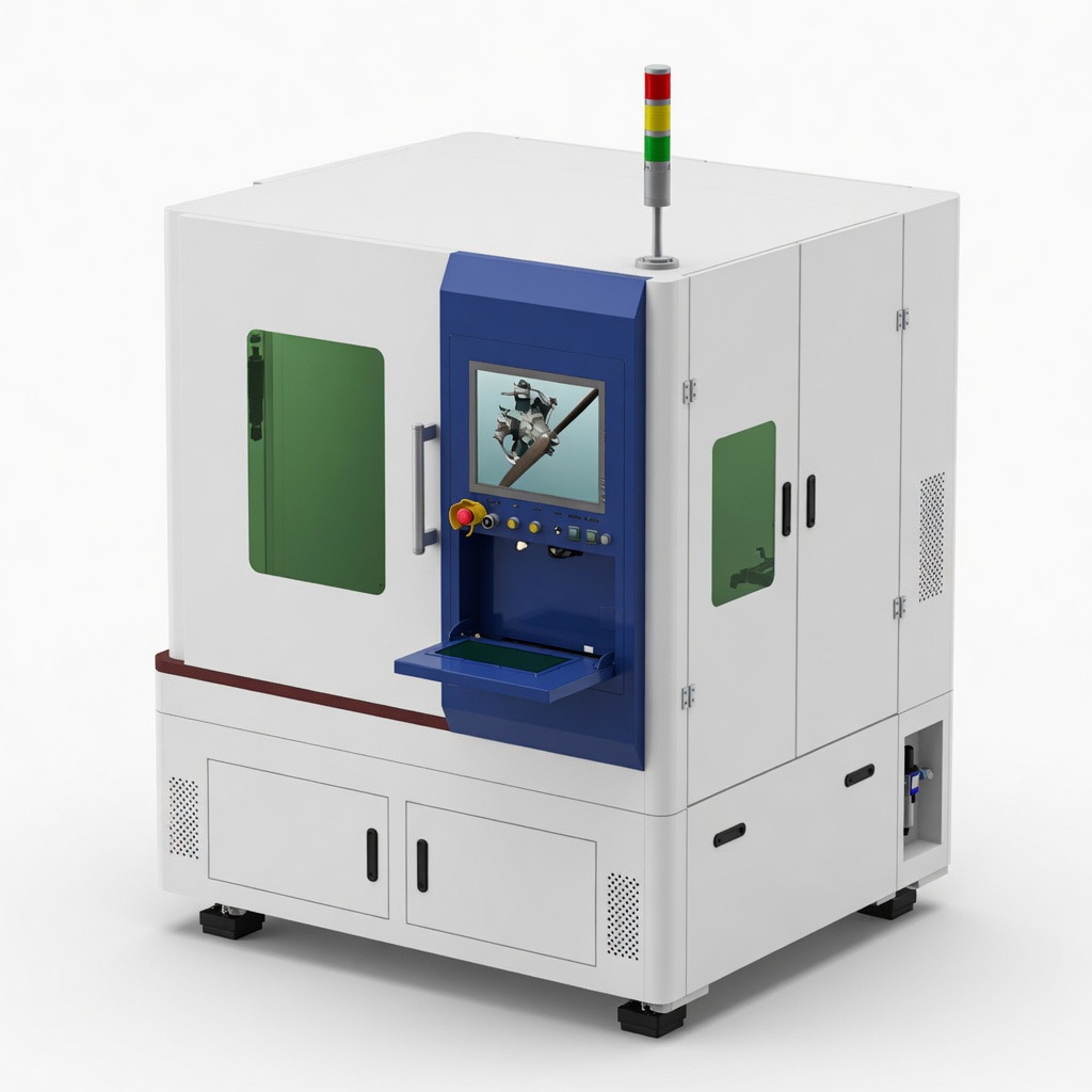
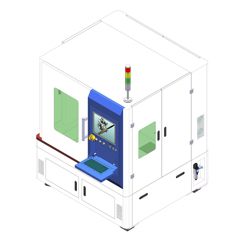
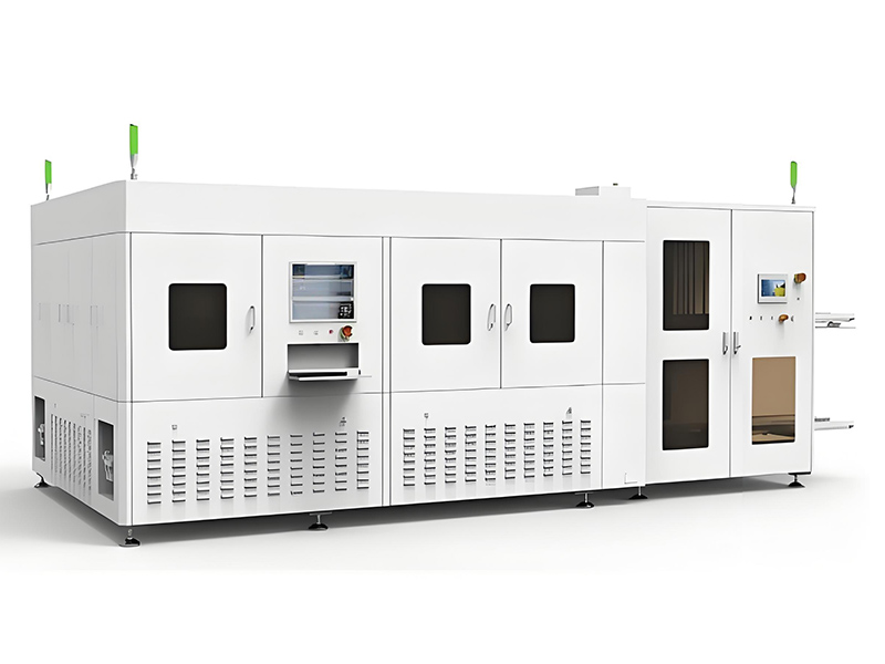
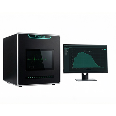
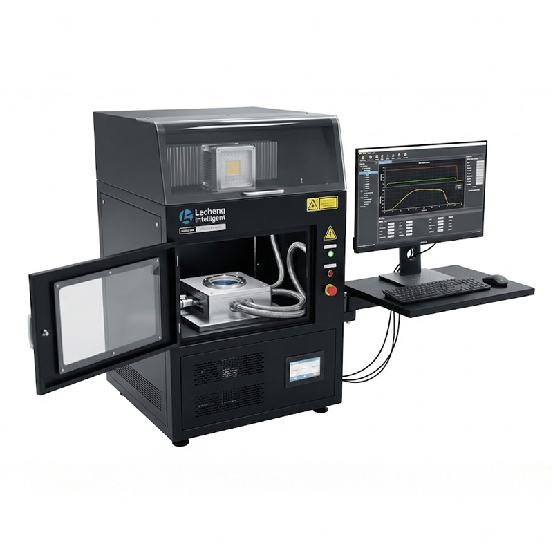
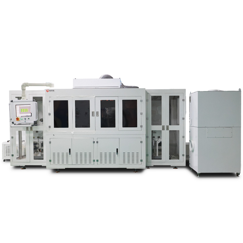
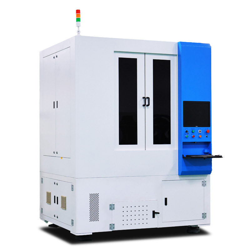
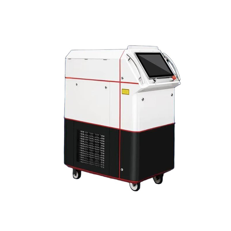
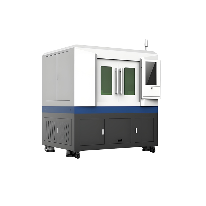
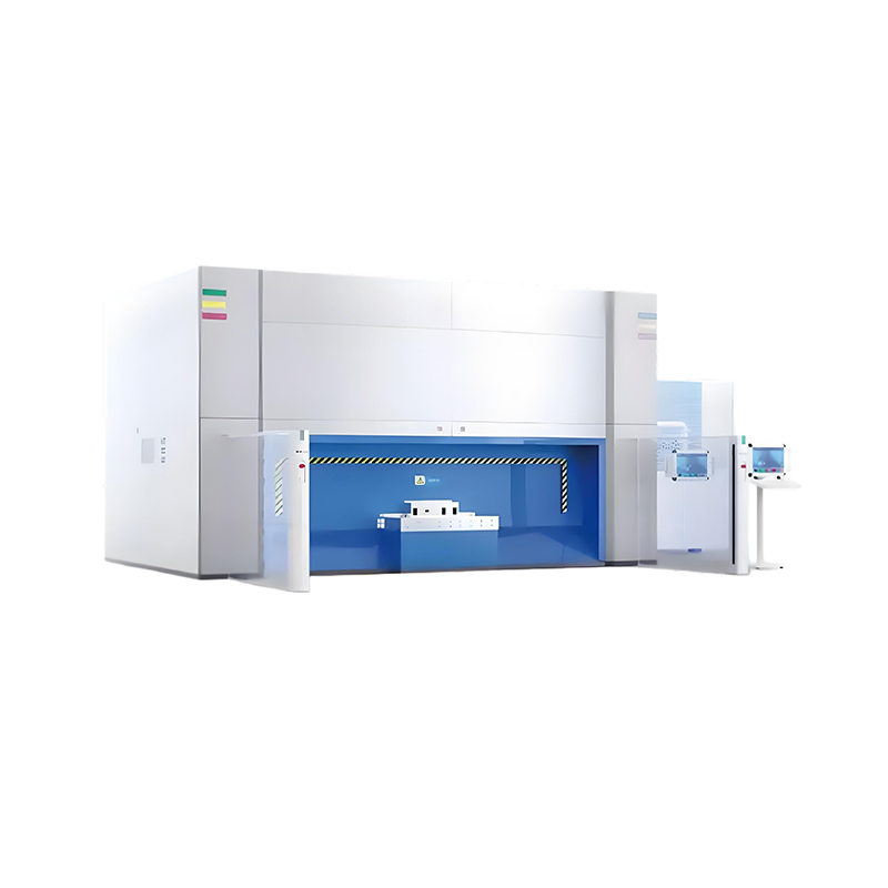
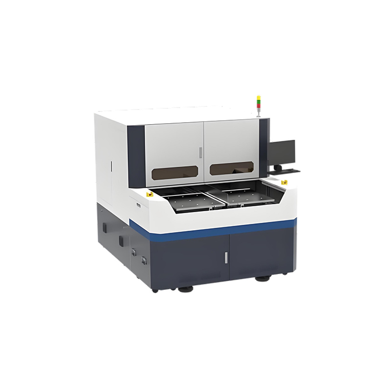
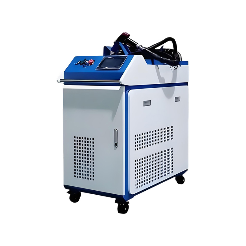
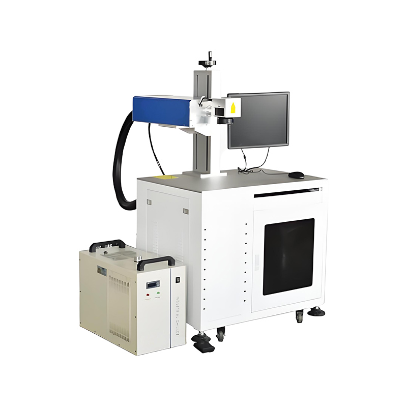
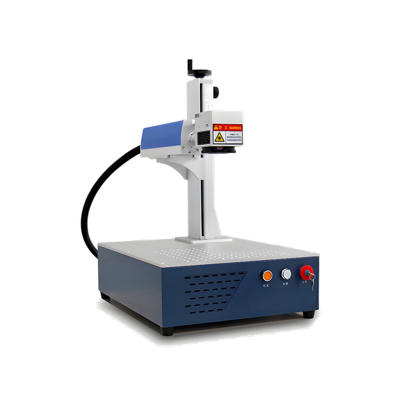
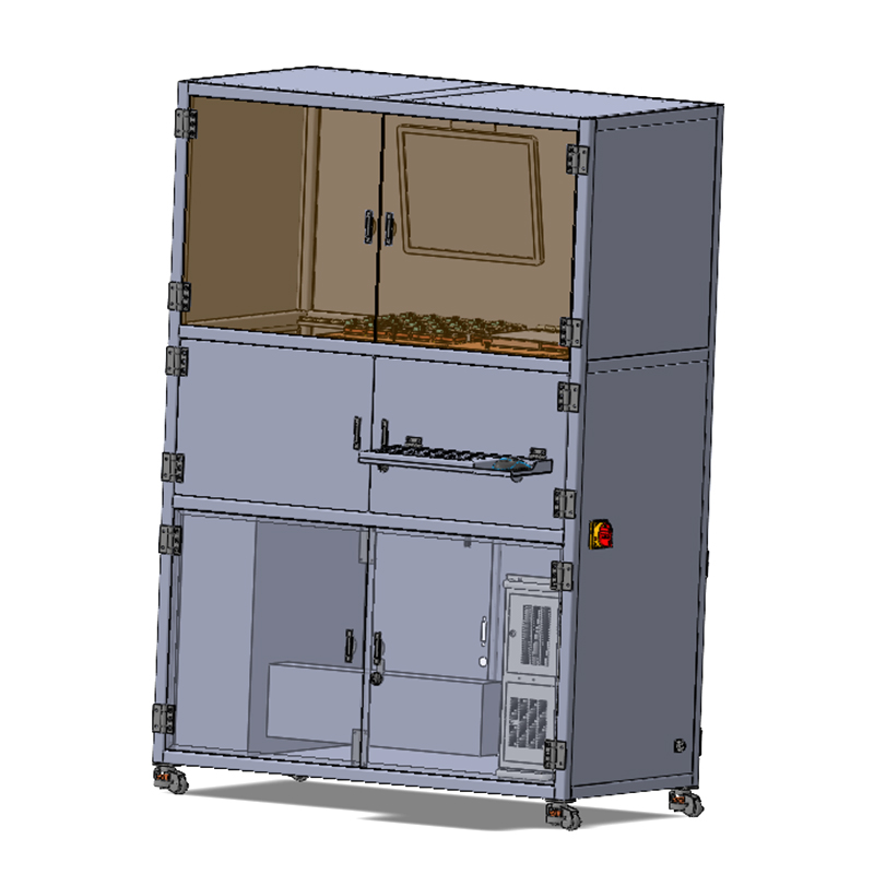
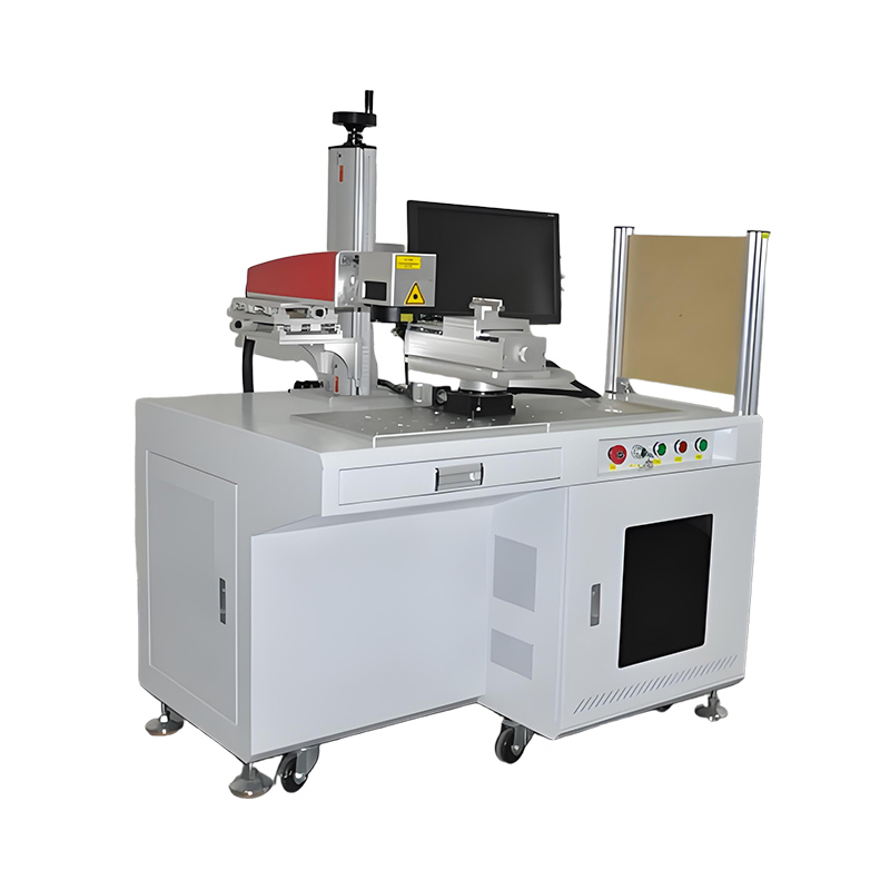
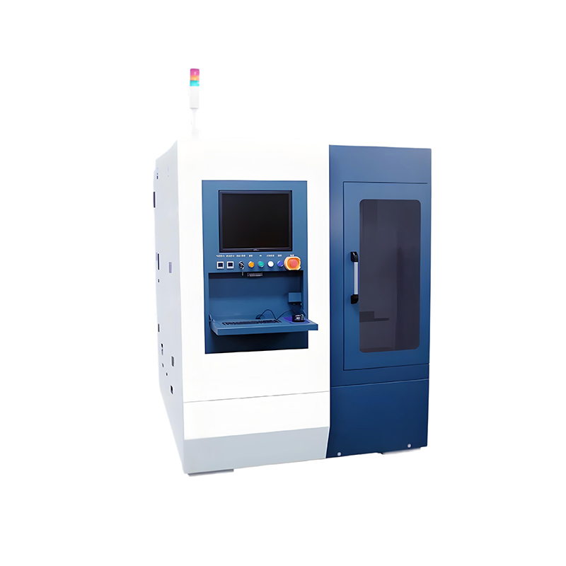
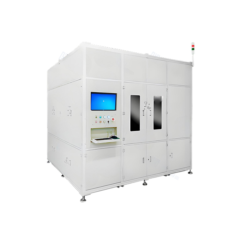
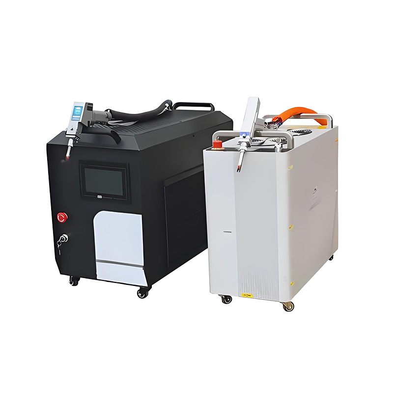
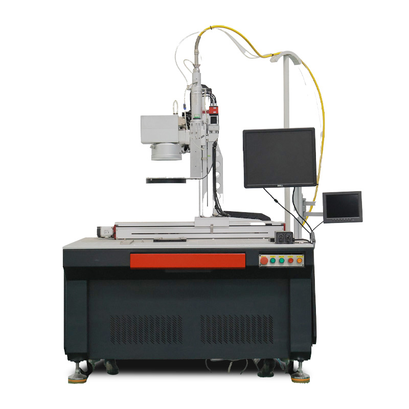
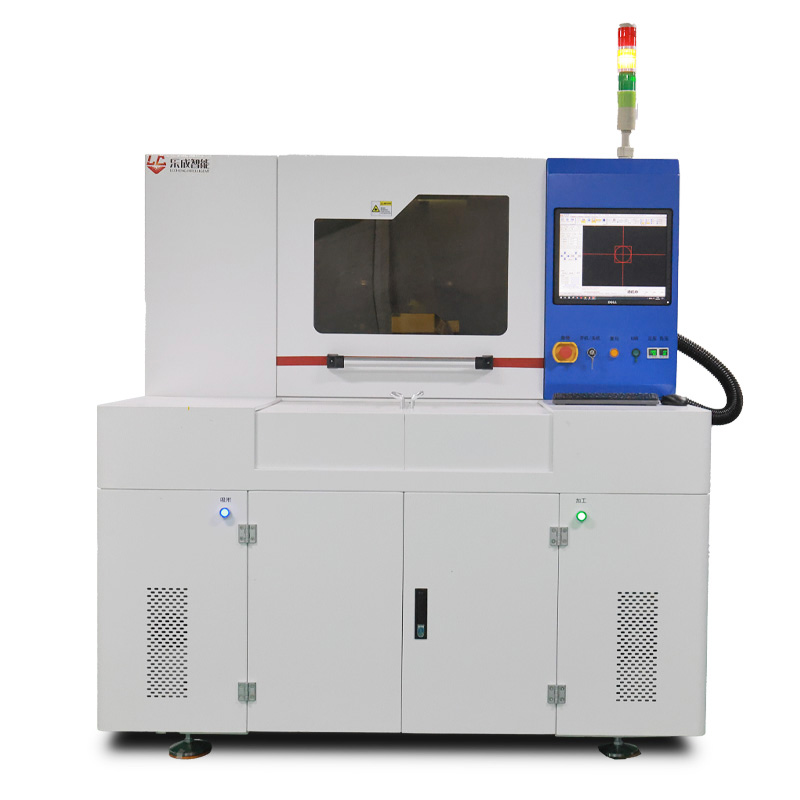
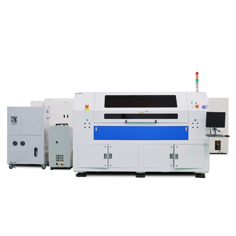
Key Characteristics for Advanced Solar Cell Manufacturing
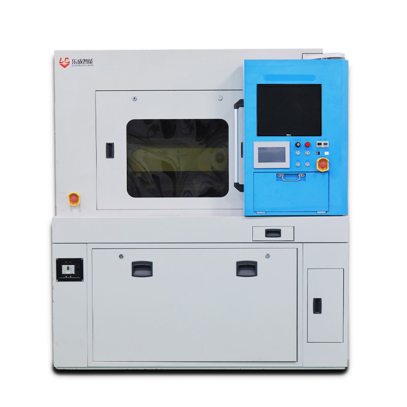
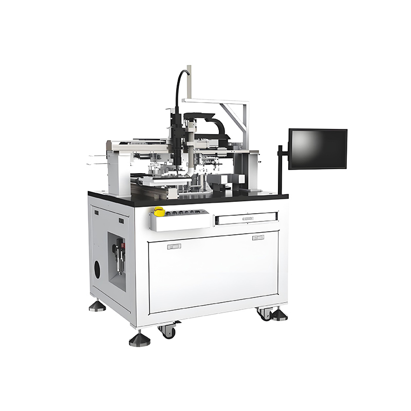
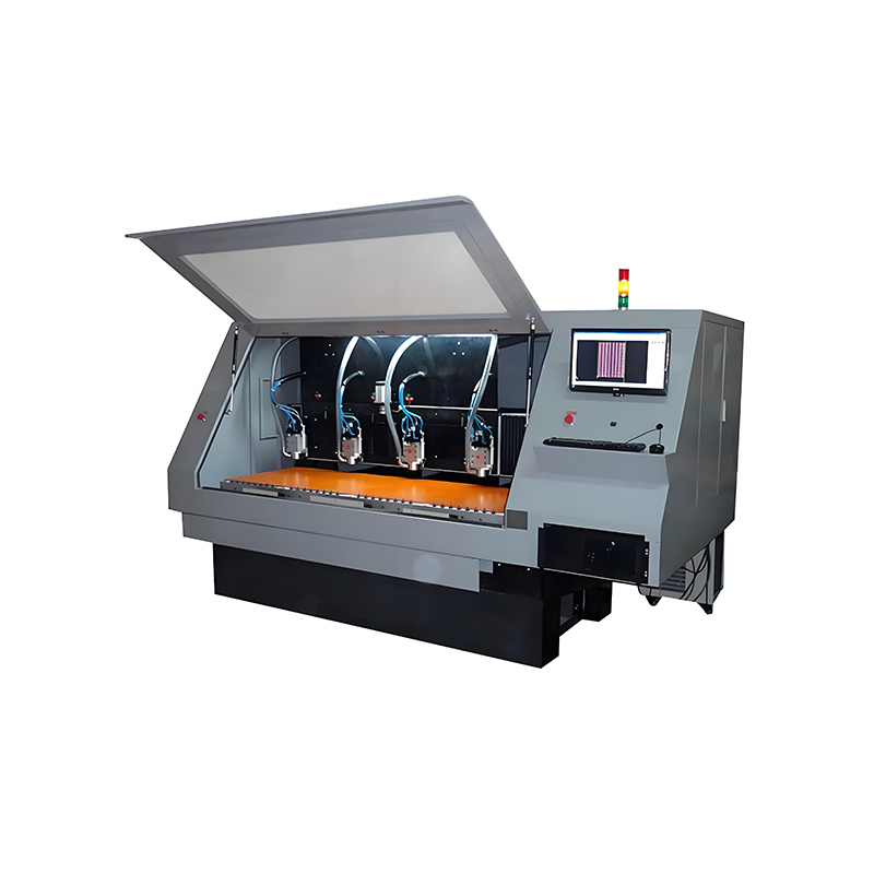
Laser scribing is a critical and precise manufacturing process in the production of thin-film solar cells, particularly perovskite photovoltaic modules. This non-contact ablation technique uses a high-energy laser beam to remove specific material layers, defining the electrical interconnection patterns that enable efficient current collection and module series interconnection. The process primarily consists of three distinct steps—P1, P2, and P3—each serving a unique function in the cell structure. Understanding the characteristics of each scribing step is essential for optimizing solar cell performance and manufacturing yield.
P1 Laser Scribing: Creating Electrical Isolation
The P1 scribing step is the first and foundational process in solar cell manufacturing. This step involves patterning the transparent conductive oxide (TCO) layer, typically composed of materials like ITO or FTO, deposited on a glass or flexible substrate. The primary objective of P1 scribing is to create electrically isolated regions that will form the basis for individual solar cell segments.
The key characteristic of P1 scribing is the requirement for complete removal of the TCO layer without damaging the underlying substrate. This precision demands careful parameter optimization, as excessive laser power can cause microcracks in the glass substrate, while insufficient power leaves conductive material residues that lead to electrical shorts between cells. Research indicates that for a 500nm thick ITO layer, optimal P1 parameters typically involve a laser power of 1.8-2.4W and scribing speeds below 2500 mm/s, resulting in trench widths of less than 10μm. The quality of P1 scribing directly impacts the geometrical fill factor (GFF), a crucial parameter determining the active area available for power generation .
P2 Laser Scribing: Establishing Series Interconnection
P2 scribing represents the most technically challenging step in the laser patterning process. This step occurs after the deposition of multiple functional layers, including the electron transport layer (ETL), perovskite absorber layer, hole transport layer (HTL), and sometimes a preliminary electrode layer. The P2 process must precisely ablate these multiple layers to expose the underlying TCO layer cleared during P1, creating a conductive pathway that series-connects the front electrode of one cell to the rear contact of the adjacent cell.
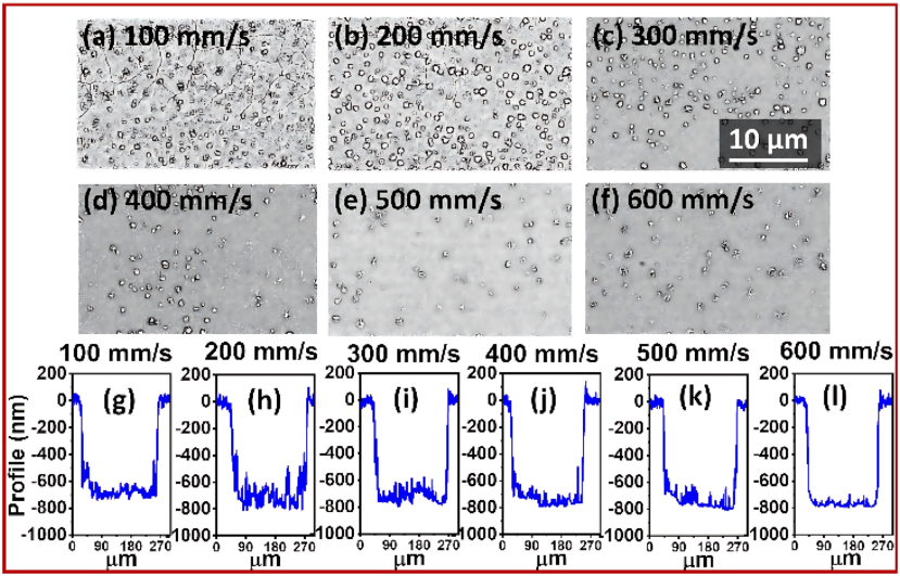
The critical challenge in P2 scribing lies in achieving sufficient depth to remove all functional layers completely without damaging the TCO layer beneath. Studies using 532nm wavelength femtosecond lasers have demonstrated success with significantly lower power settings (approximately 0.46W) compared to P1, but with higher scribing speeds (around 4000 mm/s) to minimize heat accumulation
. The P2 scribe depth must be carefully controlled—typically around 858nm for certain multilayer structures—to ensure clean ablation without underlying substrate damage . Inadequate P2 scribing can increase contact resistance, impairing current flow between adjacent cells, while excessive ablation can damage the TCO layer, creating poor electrical connections .
P3 Laser Scribing: Final Cell Isolation
The P3 scribing step completes the electrical patterning process by isolating the front contact of each individual cell. This step is performed after the deposition of the top metal electrode, typically a layer of gold or other conductive metal. The purpose of P3 is to create a trench that separates the front electrodes of adjacent cells, preventing electrical short circuits while maintaining the series connection established by the P2 process.
P3 scribing requires exceptional precision, as it must remove the metal electrode layer without damaging the underlying perovskite and charge transport layers that are critical to the cell's operation. Optimal parameters for P3 often involve even lower laser power (around 0.2W) and higher speeds (approximately 6000 mm/s) compared to previous steps, resulting in trench depths of approximately 534nm. The quality of P3 scribing is reflected in the relative performance parameters of the resulting sub-cells—when performed correctly, the separated cells should maintain nearly 100% of their original short-circuit current, open-circuit voltage, and fill factor values .
Technological Considerations and Applications
The effectiveness of all three laser scribing processes depends on several technological factors. Laser wavelength selection is critical, with fiber lasers (1064nm), Nd:YAG lasers, and ultraviolet lasers (355nm) being common choices depending on the material properties. The non-contact nature of laser scribing eliminates tool wear and mechanical stress on fragile materials, while offering micron-level precision unmatched by mechanical alternatives .
Different laser types offer distinct advantages for various applications. Fiber lasers provide high beam quality and efficiency for metal processing, while CO₂ lasers excel with organic materials. Ultraviolet lasers, with their shorter wavelength, enable higher resolution patterning essential for advanced solar cell architectures. The progression from P1 to P3 demonstrates a trend of decreasing laser power requirements but increasing need for precision and control, reflecting the growing complexity of the layered structure being processed .
Conclusion
The P1, P2, and P3 laser scribing processes each play distinct but interconnected roles in manufacturing high-efficiency thin-film solar cells. P1 establishes the foundational electrical isolation, P2 creates the critical series interconnection between cells, and P3 completes the circuit isolation. Together, these precision processes enable the production of series-connected solar modules with minimized dead areas and maximized active area for power generation. As solar cell technologies continue to advance toward higher efficiencies and thinner layer architectures, the precision and control offered by laser scribing will remain indispensable for commercial viability.
Core Keywords:
Laser scribing equipment
P1 P2 P3 laser process
Perovskite solar cell manufacturing
Precision laser ablation
Thin-film patterning
Solar cell interconnection
Non-contact material processing
High-precision laser systems

