Laser Ablation: The Core Process of Precision Marking
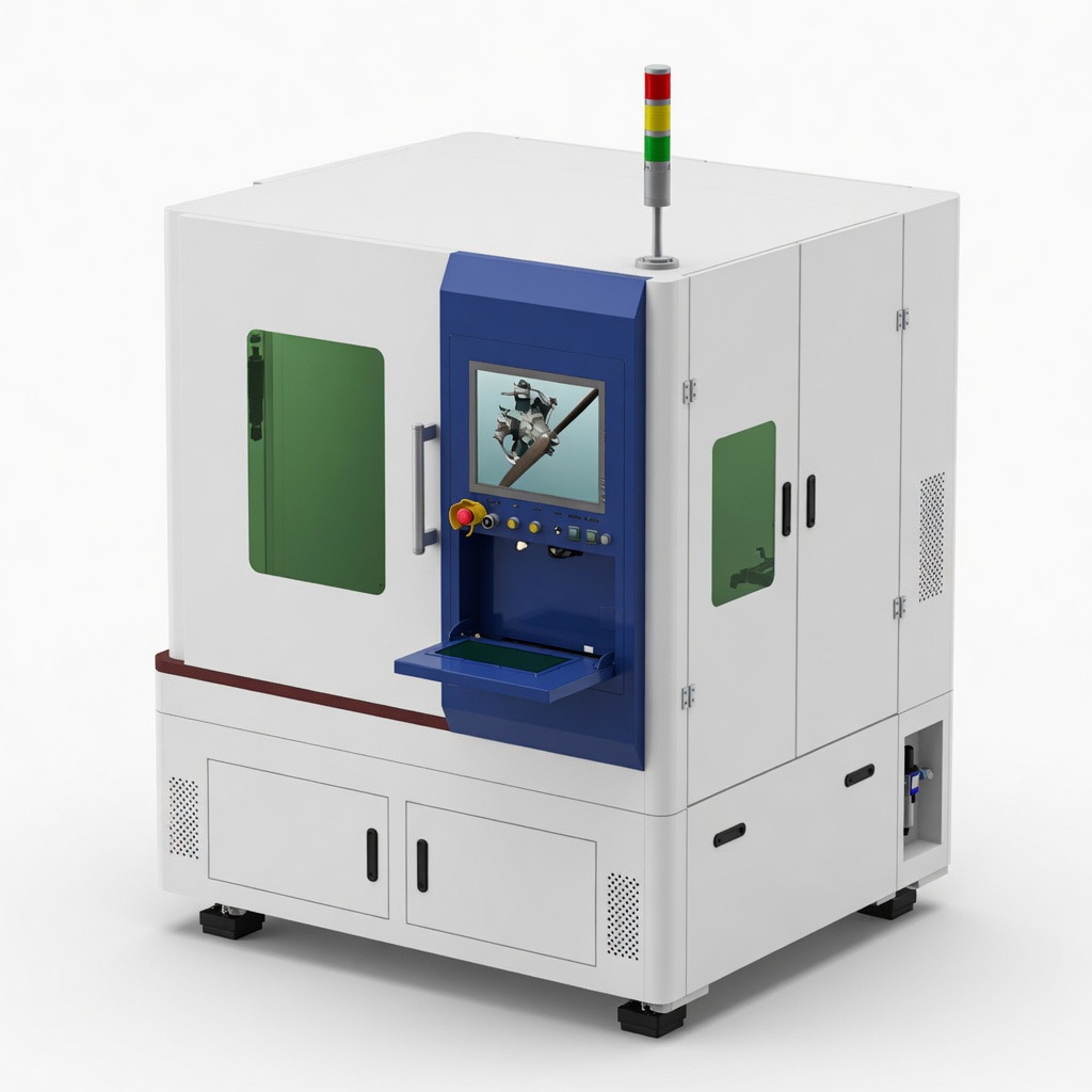
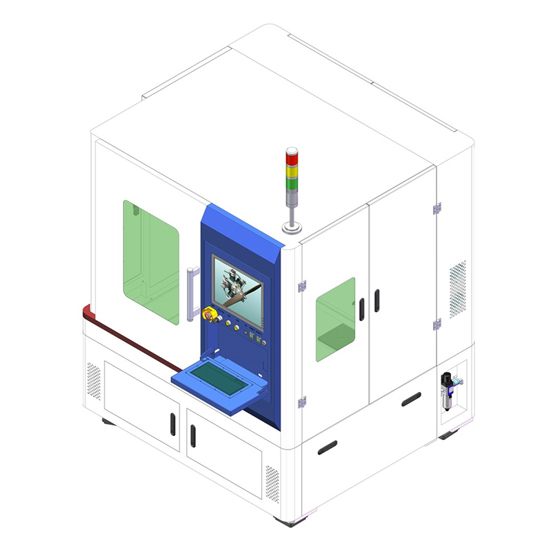
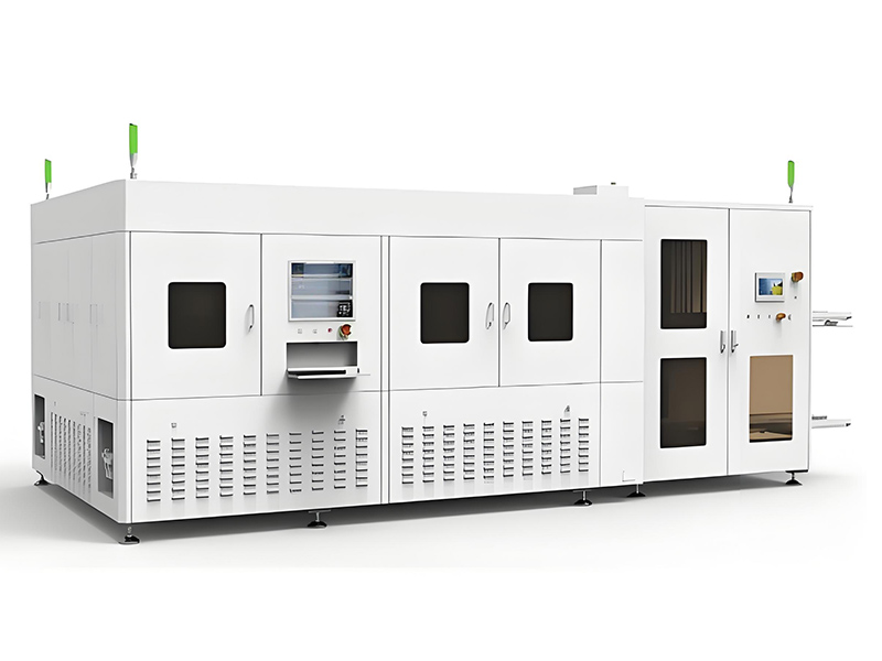
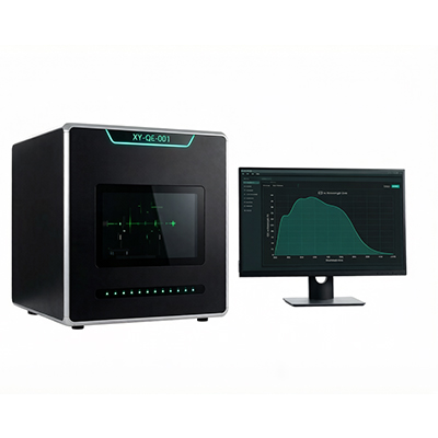
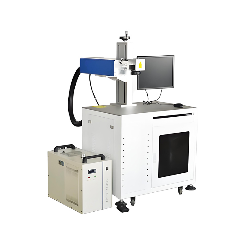
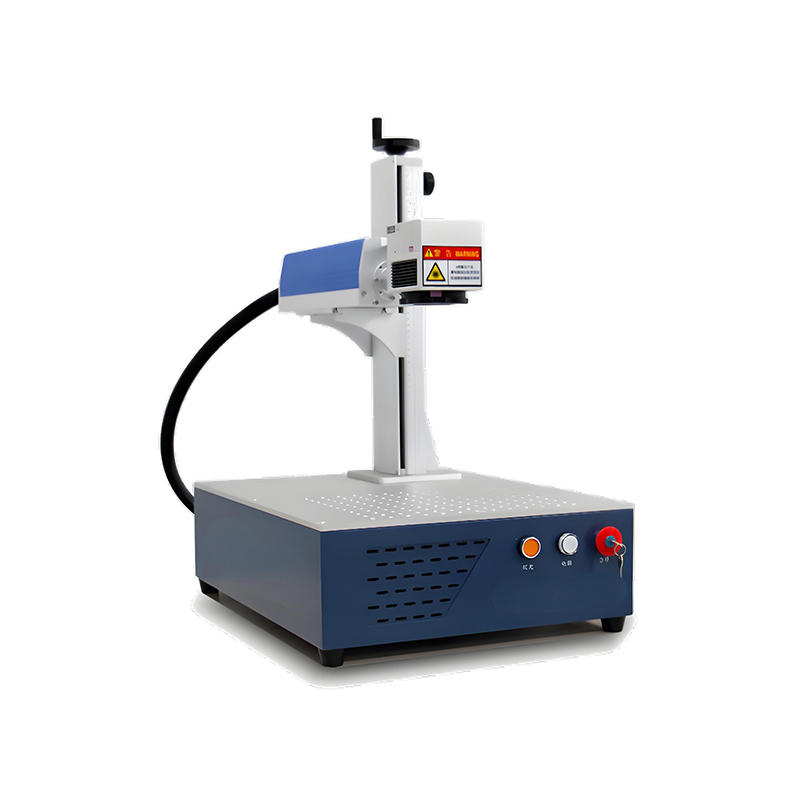
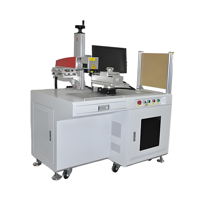
Laser ablation, a sophisticated material processing technology, has established itself as a cornerstone technique in precision marking and micro-fabrication. This process utilizes high-energy pulsed laser beams to selectively remove material from a surface through vaporization, achieving unparalleled accuracy in creating fine features and markings. As industries increasingly demand higher precision and minimal thermal impact, laser ablation continues to evolve, offering innovative solutions across various manufacturing sectors.
Fundamental Principles and Mechanisms
At its core, laser ablation involves focusing a high-energy laser beam onto a material's surface, where the photon energy is absorbed and converted into thermal energy. This rapid energy transfer causes the surface temperature to skyrocket, immediately vaporizing the material at the focal point. The process can be precisely controlled to remove thin layers of material with micron-level accuracy without affecting the surrounding areas.
The effectiveness of laser ablation depends on several critical parameters. Laser wavelength determines how different materials absorb the energy, with ultraviolet wavelengths particularly effective for many materials due to their high absorption characteristics. Pulse duration is equally crucial; shorter pulses (nanosecond to femtosecond scale) minimize heat diffusion to surrounding areas, reducing thermal damage. Additionally, pulse energy and spot size directly influence the ablation rate and feature resolution.

Different laser types yield distinct ablation characteristics. Continuous-wave lasers provide stable energy output suitable for processing non-metallic materials and polymers, while pulsed lasers excel in precision applications requiring minimal thermal impact. Ultrafast femtosecond lasers, in particular, generate extremely short pulses that ablate material so quickly that there is negligible time for heat to spread to the surrounding material, enabling "cold ablation" processes ideal for heat-sensitive applications.
Technical Advantages in Precision Marking
Laser ablation offers several compelling advantages that make it indispensable for precision marking applications. Its non-contact nature eliminates tool wear and mechanical stress on delicate workpieces, while its high spatial resolution (down to 10 micrometers or less) supports the creation of extremely fine features and markings.
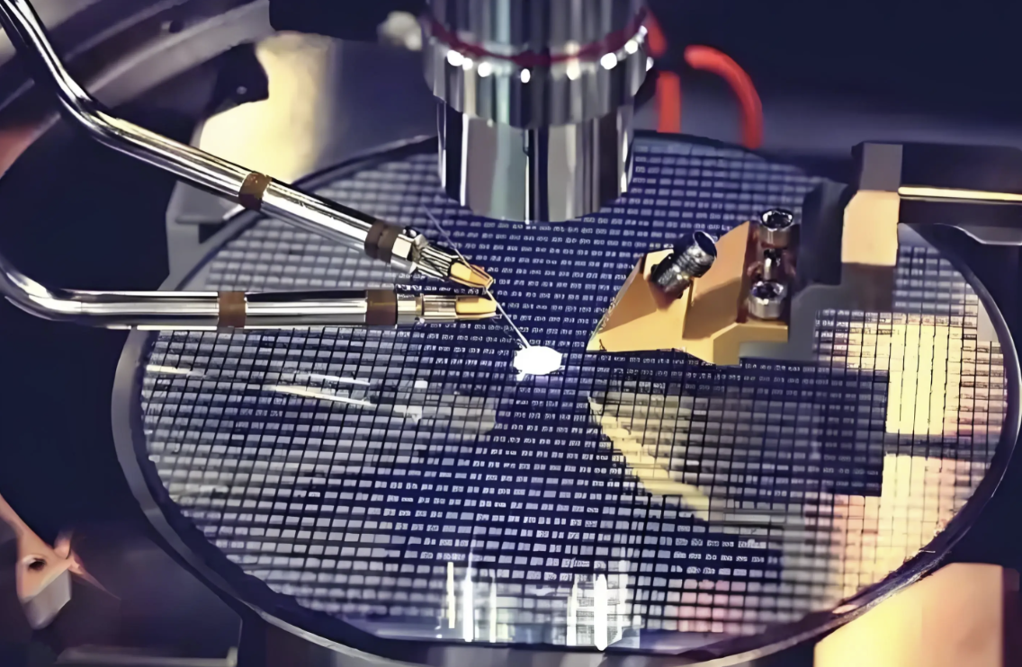
This technology provides exceptional processing flexibility through computerized control systems that can adjust parameters in real-time and handle complex designs with ease. Furthermore, it is a green manufacturing technology that typically requires no chemicals or solvents, making it environmentally friendly compared to many traditional marking methods.
The versatility of laser ablation allows it to process an extensive range of materials, from metals and semiconductors to ceramics and polymers. This adaptability makes it suitable for diverse industrial applications, from creating permanent markings on medical devices to precision patterning of electronic circuits.
Innovative Applications Across Industries
In the electronics industry, laser ablation has become critical for manufacturing high-density printed circuit boards (PCBs). The technology enables the creation of microvias and high-aspect-ratio blind holes essential for interlayer connections in compact electronic devices. Research has demonstrated techniques for creating large-aperture deep micro-blind holes using stacked hole designs, effectively doubling maximum aperture production capacity while maintaining excellent laser ablation uniformity.
The medical device field benefits significantly from laser ablation's precision capabilities. It is employed to create fine features on surgical instruments, mark medical implants with traceability codes, and texture surfaces for improved biocompatibility. The technology's minimal heat-affected zone is particularly valuable for processing temperature-sensitive biomedical materials.
In automotive and aerospace applications, laser ablation creates permanent identification marks on components for traceability and quality control. It also processes difficult-to-machine materials like carbon-fiber composites and heat-resistant superalloys, where conventional methods often prove inadequate.
Emerging applications continue to expand the technology's horizons. Laser-induced forward transfer (LIFT) techniques show promise for printing micro-scale electronic components, while laser ablation in the pharmaceutical industry enables precise drug coating removal for controlled-release formulations.
Recent Technological Advancements
Recent innovations have significantly enhanced laser ablation capabilities, particularly for challenging materials and applications. Laser-induced microjet-assisted ablation (LIMJAA) represents a notable advancement, addressing common issues like debris redeposition and heat accumulation. This technique generates continuous directional high-speed microjets through the asymmetric collapse of laser-induced cavitation bubbles in an ultra-thin liquid film environment. These microjets effectively remove secondary bubbles and ablation debris from the processing zone, resulting in higher-quality microstructures with improved material removal rates.
For hard and brittle materials like silicon carbide, traditional machining methods often cause cracks and surface damage. Laser ablation has emerged as a superior alternative, especially when combined with innovative approaches like laser-induced controllable damage-assisted grinding. This hybrid process uses laser energy to create precisely controlled surface modifications that subsequent grinding operations can easily remove, significantly improving processing efficiency and surface quality.
The development of laser ablation in liquid environments has opened new possibilities for nanomaterials preparation. Femtosecond laser microchannel liquid-phase ablation, for instance, enables the continuous production of semiconductor nanocrystals with excellent dispersion properties. This method separates the ablation and surface coating processes into distinct but connected steps, effectively preventing nanoparticle agglomeration while avoiding the amorphous carbon coating issues that plague conventional methods.
Future Outlook
As manufacturing demands continue to evolve toward smaller features, more complex materials, and higher precision requirements, laser ablation technology is poised to play an increasingly vital role. Future developments will likely focus on improving processing speeds through higher-power ultrafast lasers, enhancing quality control with real-time monitoring systems, and expanding the range of processable materials through wavelength diversification and pulse shaping technologies.
The integration of artificial intelligence for process optimization and the development of hybrid approaches that combine laser ablation with complementary technologies will further expand the applications of this versatile precision manufacturing method. As these advancements materialize, laser ablation will continue to solidify its position as an essential technology for precision marking and micro-fabrication across countless industries.

