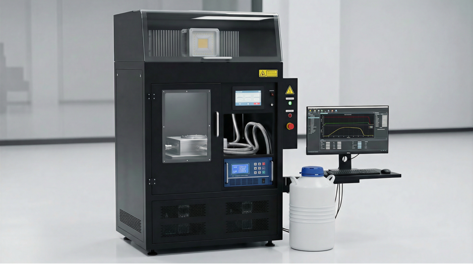
Cell Laser Scribing Machine")


 Co., Ltd.")
Laser Ablation vs. Engraving vs. Cutting: A Technical Comparison of Processes and Applications
Laser processing technologies, including ablation, engraving, and cutting, are fundamental to modern precision manufacturing. While they all utilize high-energy laser beams to interact with materials, they are distinguished by their core objectives, key process parameters, and resultant application scenarios. Understanding these differences is crucial for selecting the appropriate technology for specific industrial needs.

1. Fundamental Principles and Core Objectives
The primary distinction lies in the intended outcome and the physical interaction with the material.
Laser Ablation: The core objective of laser ablation is the precise,微量 (micro-scale) removal of material to achieve surface modification or create micro-structures. It often employs ultra-short pulses (picosecond or femtosecond) to deposit energy so rapidly that the material transitions directly from a solid to a plasma (sublimation), minimizing the Heat-Affected Zone (HAZ). This "cold processing" mechanism is ideal for applications where thermal damage to the surrounding material must be avoided, such as in the fabrication of micro-electronics or medical device surface functionalization. The goal is not just removal, but controlled modification at a microscopic level.
Laser Engraving: This process aims to create visible marks, patterns, or textures on a material's surface. It typically uses continuous-wave or longer pulsed lasers (e.g., nanosecond) to melt, vaporize, or induce a chemical reaction in a shallow surface layer. The depth of removal is greater than mere marking but is not intended to fully penetrate the workpiece. The key parameters are contrast, legibility, and aesthetic appearance, making it suitable for branding, serial numbers, and decorative work on metals, plastics, and leather.

Laser Cutting: The goal of laser cutting is the complete separation of a material along a defined path. It utilizes high average power to melt or vaporize the material through its entire thickness, often assisted by a gas jet to eject molten residue. Key parameters include cutting speed, edge perpendicularity, and minimal slag formation. It is characterized by its ability to profile sheets of metal, plastic, or composites with high precision and speed, replacing mechanical punching or sawing in many applications.

2. Technical Parameter Comparison and Resultant Effects
The different objectives dictate significant variations in their key technical parameters.
The table below summarizes the critical distinctions in their process configurations:
Feature | Laser Ablation | Laser Engraving | Laser Cutting |
|---|---|---|---|
Primary Goal | Micro-scale removal, surface modification, micro-structuring | Creating surface marks, patterns, or textures | Complete material separation, contouring |
Depth/Material Interaction | Nanometers to micrometers; achieves surface modification through vaporization/sublimation. | Micrometers to millimeters; melts or vaporizes a surface layer. | Full penetration; melts/burns through the entire thickness. |
Key Process Parameters | Ultra-short pulses (pico/femtosecond), high peak power density, high-precision scanning control. | Lower power density, adjustable scanning speed and hatch spacing. | High average power, slower scanning speed (relative to engraving), type and pressure of assist gas. |
Heat-Affected Zone (HAZ) | Extremely small or nonexistent ("cold working"), causing almost no damage to surrounding material. | Relatively small, but some thermal effect like discoloration may occur. | Significant, results in a noticeable HAZ, often with slag or thermal deformation. |
Spatial Resolution | Very high (can be less than 10µm), suitable for creating fine micro-features. | Moderate to high, depends on spot size and material. | Defined by the kerf width (cutting slit), which is larger than ablation/engraving spots. |
3. Application Scenarios: From Microelectronics to Macro-Fabrication
The unique capabilities of each process determine their dominant application areas across industries.
Laser Ablation Applications: Its precision makes it indispensable in high-tech sectors.
Electronics & Semiconductors: Trimming resistors, creating micro-vias on circuit boards, and insulating thin-film solar cells.
Medical Device Manufacturing: Processing cardiovascular stents, creating micro-features on surgical tools, and texturing surfaces for improved biocompatibility with minimal thermal impact.
Aerospace: Producing micro-cooling holes in turbine blades and structuring surfaces for reduced friction.
Laser Engraving Applications: This technology is versatile for surface marking and personalization.
Product Identification: Permanent marking of serial numbers, barcodes, and logos on machine parts, consumer goods, and tools.
Personalized Gifts: Customizing designs on items made of wood, glass, acrylic, and leather.
Mold & Die Texturing: Creating textured surfaces on molds for plastic injection or sheet metal forming to impart specific surface finishes to the final product.
Laser Cutting Applications: It is a versatile solution for shaping sheet materials.
Industrial Manufacturing: Profiling automotive body parts from sheet metal, cutting components for electronic enclosures, and processing carbon fiber composites for aerospace.
Advertising & Signage: Intricately cutting letters and shapes from acrylic, wood, and composite panels.
Textile & Apparel: Precisely cutting fabrics, leather for shoes and garments, and technical textiles with sealed edges to prevent fraying.
In summary, the choice between laser ablation, engraving, and cutting is a function of the desired outcome: microscopic modification or structuring, surface marking, or complete separation. Advances in ultra-fast lasers continue to blur the lines, particularly between high-quality ablation and engraving, pushing the boundaries of precision manufacturing across all sectors.