Precision Requirements of P1, P2, P3 Laser Scribing Processes and Their Impact on Final Cell Efficiency
The precision of the P1, P2, and P3 laser scribing processes is fundamental to the high-efficiency operation of perovskite solar cells. The table below summarizes the core objectives, key precision control elements, and the direct impact of each process on the final cell efficiency.
Process Step | Core Objectives & Precision Requirements | Key Impact on Cell Efficiency |
|---|---|---|
P1 (Back Electrode Isolation) | Objective: Precisely ablate the Transparent Conductive Oxide (TCO) layer to form insulated stripes on the substrate. | 1. Lays the foundation for Geometric Fill Factor (GFF): The position and width of the P1 line serve as the baseline for subsequent P2 and P3 lines, directly determining the initial size of the "dead area." |
P2 (Forming Interconnection) | Objective: Precisely ablate the perovskite absorber layer and hole transport layer to expose the underlying P1 TCO, creating a series connection. This is the most technically challenging step. | 1. Determines series resistance: Incomplete P2 scribing (residue) increases contact resistance between sub-cells; overscribing that damages the TCO destroys the conductive channel, both leading to a reduced Fill Factor (FF) and output voltage. |
P3 (Top Electrode Isolation) | Objective: Remove the metal top electrode and underlying functional layers to achieve electrical isolation of the sub-cells, completing the series circuit. | 1. Completes electrical isolation: Incomplete P3 scribing can cause the top electrodes of adjacent sub-cells to short-circuit, rendering the entire module ineffective. |
💡 In-Depth Understanding of the Precision-Efficiency Relationship
Beyond the direct requirements outlined in the table, the ultimate impact on cell efficiency hinges on several interconnected factors managed through precision scribing.
Dead Area and Geometric Fill Factor (GFF): The P1, P2, and P3 lines, along with the safe spacing between them, collectively form the non-electricity-generating "dead area." The total area of the dead zone directly determines the module's "Geometric Fill Factor (GFF)." Maximizing the effective generation area (i.e., minimizing the dead area) is a crucial lever for boosting the overall output power of a module, assuming a given conversion efficiency of the perovskite material itself. One analysis suggests that for a 1.0m × 2.0m module, reducing the dead area width from 250 μm to 130 μm can increase the output power per module by approximately 8.47 watts (assuming an active area efficiency of 18%), translating to significant additional revenue for GW-scale production lines.

Thermal Impact and Material Damage: Laser processing inherently involves energy interaction with the material. Poorly controlled energy (e.g., using traditional nanosecond lasers) can create a Heat Affected Zone (HAZ) that alters the crystal structure of the perovskite material, introducing defects that act as recombination centers for charge carriers (photogenerated electrons and holes), thereby reducing the cell's open-circuit voltage and short-circuit current. Consequently, the industry trend is towards using ultrafast lasers (e.g., picosecond, femtosecond). Their "cold processing", enabled by extremely high peak power that causes instantaneous material vaporization, reduces the HAZ to the micrometer or even nanometer scale, better preserving the optoelectronic properties of the perovskite material .
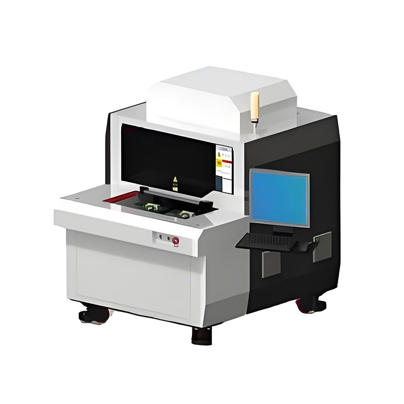
Online Monitoring and Process Control: In large-area mass production, ensuring consistency across thousands of scribed lines is paramount. Advanced manufacturing systems integrate online vision inspection systems. These systems can realistically track the actual position of the P1 reference line (compensating for minor substrate deformation in subsequent processes) and dynamically adjust the scribing paths for P2 and P3, ensuring the line spacing remains within the set range. For example, by setting safety thresholds, the system can alarm when spacing anomalies occur, helping to keep the dead area consistently optimized while avoiding line intersections and short circuits.
💎 Conclusion
The precision of the P1, P2, and P3 laser scribing processes is the cornerstone of high-efficiency perovskite solar cells. The precise positioning of the P1 line is the foundation, the selective etching of the P2 line is the most difficult challenge, and the complete isolation by the P3 line is the final safeguard. They collectively act upon three core dimensions: minimizing the dead area, reducing series resistance, and avoiding thermal damage to the material. These factors ultimately determine the module's Geometric Fill Factor, series resistance, and carrier collection efficiency, significantly impacting its final photoelectric conversion efficiency and output power. With advancements in ultrafast laser technology and intelligent online monitoring systems, the precision and efficiency limits of perovskite cell manufacturing continue to be pushed higher.
I hope this translation is helpful. Should you have further interest in specific topics, such as a comparison of different laser types (e.g., UV nanosecond vs. green picosecond) or more detailed failure modes, I am ready to continue the discussion.

