


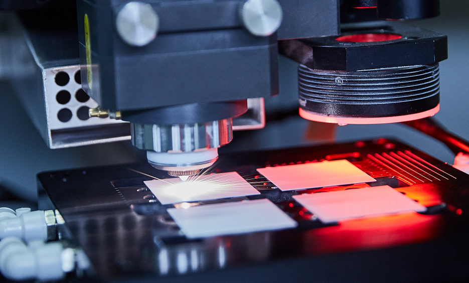
Femtosecond Laser Processing
Femtosecond laser processing represents one of the most advanced frontiers in precision manufacturing today. This technology utilizes laser pulses of incredibly short duration—approximately 10⁻¹⁵ seconds—to achieve material processing with unparalleled precision and minimal thermal damage. The unique characteristics of femtosecond lasers have opened up revolutionary possibilities across industries from medical devices to aerospace engineering.

The Physics Behind Femtosecond Laser Processing
The extraordinary capabilities of femtosecond lasers stem from fundamental physical principles. The interaction between femtosecond laser pulses and materials is an ultrafast nonlinear and non-equilibrium process. Unlike traditional long-pulse lasers where the laser pulse duration exceeds thermal diffusion time, femtosecond lasers operate on a timescale shorter than the electron-lattice energy transfer (approximately 1-10 picoseconds) .
This temporal characteristic enables what scientists call "cold processing" or "non-thermal processing". When a femtosecond laser pulse interacts with a material, electrons absorb photon energy and heat rapidly due to their low specific heat capacity. The surface material undergoes instantaneous ionization and ejection before thermal energy can diffuse to the surrounding area . This mechanism prevents the formation of a heat-affected zone (HAZ), recast layers, micro-cracks, and other thermal damage that plague conventional laser processing .
The extremely high peak power of femtosecond lasers (exceeding 10¹² W/cm²) enables nonlinear absorption processes including multi-photon ionization and tunneling ionization. These effects allow processing of virtually any material, including transparent substrates, by overcoming their natural bandgaps without linear absorption .
Key Advantages and Technological Capabilities
1. Ultra-High Precision Processing
Femtosecond lasers achieve sub-micron machining accuracy. Through techniques like two-photon polymerization (TPP), they can create structures with resolutions beyond the diffraction limit, down to 100 nanometers . This exceptional precision enables fabrication of complex 3D micro- and nanostructures impossible with traditional methods .

2. Universal Material Compatibility
A significant advantage of femtosecond lasers is their ability to process nearly all types of materials, including metals, semiconductors, dielectrics, ceramics, and polymers. This versatility eliminates the need for multiple processing systems for different materials.
3. Three-Dimensional Fabrication Capability
The nonlinear absorption of femtosecond lasers allows 3D processing inside transparent materials when tightly focused. This enables the creation of embedded waveguides, microfluidic channels, and other internal structures without surface opening .
Transformative Applications Across Industries
Medical Device Manufacturing
In healthcare, femtosecond lasers enable fabrication of bioresorbable vascular stents with precision cuts as fine as 20 micrometers. They can create surgical instruments with zero-taper holes for neurological catheters, significantly improving surgical outcomes . The technology also facilitates production of lab-on-chip devices and biosensors for advanced diagnostics .
Aerospace and Automotive Engineering
The aerospace industry relies on femtosecond lasers for machining turbine blade cooling holes in high-temperature superalloys with exceptional accuracy (5μm tolerance) and minimal taper (<1°). This processing enhances cooling efficiency and component longevity. In automotive applications, the technology enables precise manufacturing of fuel injectors with optimized spray patterns for improved combustion efficiency .
Optics and Photonics
Femtosecond lasers fabricate advanced optical components including micro-lens arrays, photonic crystals, waveguides, and diffraction gratings. These components enable developments in augmented reality displays, telecommunications, and sensing technologies .
Electronics and Semiconductor Manufacturing
The technology plays a crucial role in semiconductor processing, enabling precision dicing of brittle materials like silicon carbide wafers with minimal chipping (<5μm). It also facilitates fabrication of through-silicon vias (TSVs) with exceptional aspect ratios exceeding 20:1.
Future Perspectives and Challenges
As femtosecond laser technology continues to evolve, several trends are shaping its future development. The integration of machine learning algorithms for real-time process optimization promises to achieve "first-part-correct" manufacturing. The emergence of more affordable fiber-based femtosecond laser systems is making the technology accessible to a broader industrial base .
Current research focuses on improving processing throughput through parallelization techniques while maintaining precision. Hybrid approaches that combine femtosecond laser processing with other methods like electrochemical machining are enabling simultaneous achievement of micron-scale precision and millimeter-scale structural efficiency .
Despite significant progress, challenges remain in scaling up processing speeds for industrial-scale applications and further reducing system costs. Nevertheless, as precision manufacturing demands continue to increase across sectors, femtosecond laser processing is poised to become an increasingly indispensable technology in the Industry 4.0 landscape, enabling innovations from quantum computing devices to next-generation medical implants.

The unique combination of exceptional precision, minimal thermal impact, and universal material compatibility makes femtosecond laser processing a transformative technology that continues to push the boundaries of what is possible in advanced manufacturing.
Related product and article resources
For procurement comparison and technical evaluation, readers can continue with these related product pages and supporting articles.
- Products
- Product catalog
- Contact the sales team
- Contact us
- Laser Scribing Machine RFQ Checklist for PV Cell Production Lines
- Laser Scribing vs Mechanical Cutting in Photovoltaic Production
- P1, P2 and P3 Laser Scribing: What Solar Manufacturers Should Know
- Lecheng Powers Dehu's 100MW Perovskite Pilot Line to Historic First Light