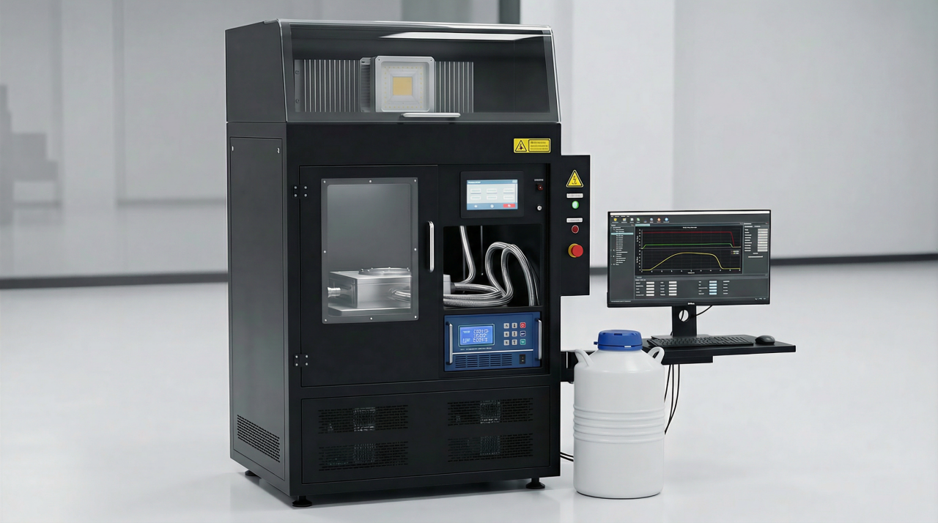
Cell Laser Scribing Machine")


 Co., Ltd.")
Ultrafast Laser Processing for Next-Generation Thin-Film Solar Cells
The evolution of thin-film photovoltaic manufacturing increasingly relies on advanced laser processing technologies. Among these, ultrafast lasers, particularly picosecond and femtosecond systems, have emerged as transformative tools for structuring and optimizing solar cells based on materials like CIGS (Copper Indium Gallium Selenide) and perovskite. Their unique ability to deliver extreme precision with minimal thermal impact addresses critical challenges in processing these often-sensitive materials, directly contributing to enhanced device performance and longevity.

The Superiority of Picosecond and Femtosecond Lasers
The fundamental advantage of ultrafast lasers lies in their pulse duration. Emitting incredibly short bursts of light measured in picoseconds (10⁻¹² seconds) or femtoseconds (10⁻¹⁵ seconds), these lasers deposit energy into a material far more rapidly than the time required for heat to diffuse into the surrounding area. This results in an ablation mechanism that is primarily non-thermal, characterized by direct solid-vapor transition. Consequently, the Heat Affected Zone (HAZ) is drastically reduced or eliminated entirely.
This is a significant improvement over traditional nanosecond lasers, whose longer pulses inevitably cause melting, cracking, and undesirable thermal effects along the processed edges. For multilayer thin-film stacks where each layer is only microns thick and possesses distinct thermal and optical properties, this precision is not just beneficial—it is essential for creating clean, electrically optimal features.
Strategic Wavelength Selection for Material-Specific Processing
The effectiveness of laser processing is equally dependent on selecting the appropriate laser wavelength, as it determines how light interacts with the different material layers. The goal is often to selectively ablate a specific layer without damaging the underlying substrate or adjacent films. This requires a wavelength that is strongly absorbed by the target material but transmitted by the others.
For example, green lasers (532 nm) are highly effective for patterning the absorber layer in structures like CIGS on a transparent conductive oxide (TCO) front electrode. The green light passes through the TCO (which is typically transparent to visible light) and is strongly absorbed by the CIGS layer, enabling precise patterning. Conversely, ultraviolet (UV) lasers (e.g., 343 nm) offer high photon energy and are readily absorbed by a wide range of materials—including polymers, metals, and semiconductors—enabling clean ablation with minimal penetration depth and superior feature definition . This makes them ideal for delicate processes on flexible polymer substrates or for defining intricate patterns on brittle materials.

Application and Performance in Key Solar Materials
The combination of ultrafast pulses and strategic wavelength selection unlocks high-quality processing for leading thin-film technologies:
CIGS Solar Cells: In the monolithic interconnection of CIGS modules, three patterning steps (P1, P2, P3) are required. Using nanosecond lasers for these steps can cause thermal damage, including micro-cracks, edge burrs, and the undesirable diffusion of elements like molybdenum (Mo) and CIGS. This can lead to shunting and reduced efficiency. Picosecond lasers, with their minimal HAZ, produce cleaner, more electrically isolated scribes. Research has demonstrated that picosecond lasers enable the creation of well-defined grooves with straight sidewalls on flexible polyimide (PI) substrates, which is difficult to achieve with mechanical scribing or nanosecond lasers due to the substrate's flexibility and thermal sensitivity.
Perovskite Solar Cells: Perovskites are notoriously sensitive to heat and environmental factors. Ultrafast lasers are pivotal for both patterning and defect engineering. For instance, excimer lasers (a type of UV laser) with high single-pulse energy have been used to irradiate perovskite films, significantly reducing their surface defect density and thereby improving the efficiency and stability of the resulting solar cells. The non-thermal nature of ultrafast ablation is crucial for patterning perovskite layers without decomposing the organic-inorganic hybrid material, preserving their excellent optoelectronic properties.
Future Outlook and Challenges
The trajectory of laser technology in photovoltaics points toward wider adoption of ultrafast systems. The primary challenge remains the initial capital investment, which is higher than for nanosecond-based systems. However, this is increasingly offset by gains in production yield, device efficiency, and process reliability. Future developments will likely focus on increasing the power and throughput of ultrafast lasers to make them more economical for mass production, as well as on refining beam-delivery systems for even greater precision and speed.
In conclusion, ultrafast laser processing, underpinned by precise control over pulse duration and wavelength, has become an indispensable technology for advancing thin-film photovoltaics. By enabling cold ablation and material-specific interactions, it allows manufacturers to push the efficiency and durability boundaries of next-generation solar cells like CIGS and perovskites, bringing us closer to more powerful and sustainable solar energy solutions.