

Laser Scribing in Perovskite Solar Module Production: P1, P2, P3 Explained
Perovskite photovoltaics move from lab records to factory lines through one deceptively narrow gate: laser scribing. The three patterning steps — P1, P2, P3 — turn a full-area thin-film stack into series-connected cells, and they set both the module voltage and the dead-area losses that separate a champion module from an average one. Here is what each step does and where production lines win or lose efficiency.
1. Why monolithic interconnection needs three scribes
A thin-film module is not assembled from separate cells; it is one large stack divided into strips connected in series. P1 cuts the bottom transparent conductor into isolated segments; P2 opens the perovskite absorber to let the top electrode contact the bottom conductor of the neighboring cell; P3 separates the top electrode. Together they form the series interconnect — and every micron of scribe width plus the spacing between P1-P2-P3 is dead area generating no power.
2. The efficiency arithmetic of dead area
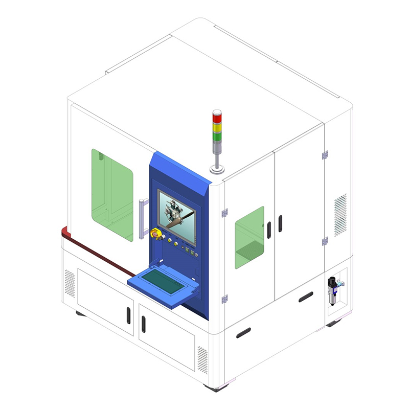
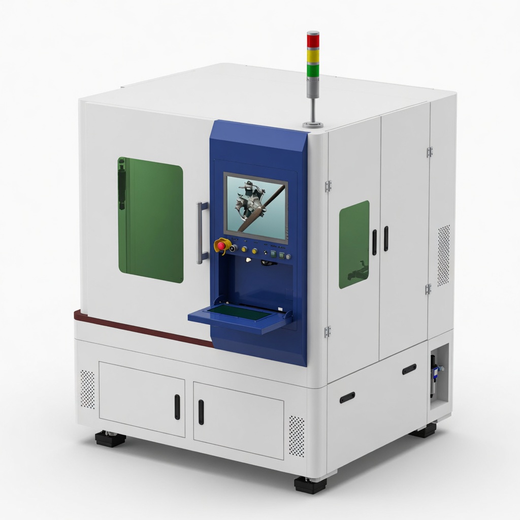
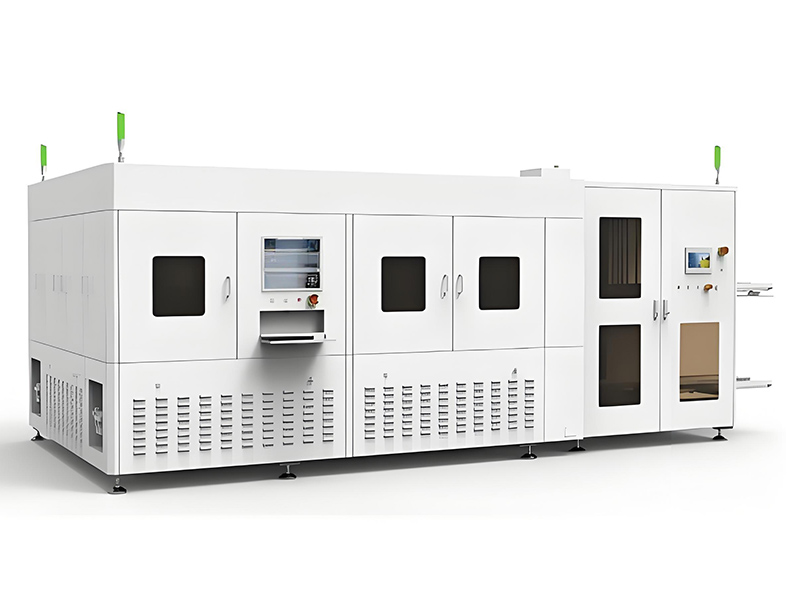
Typical interconnect zones run 100-300µm wide. On a 10mm cell pitch, a 200µm dead zone costs 2% absolute in geometric fill factor — before any electrical losses. Narrowing the zone demands tighter scribe placement accuracy (±5µm class), smaller spot sizes, and vision-guided alignment between steps, which is exactly where purpose-built scribing platforms, like Lecheng production systems, differentiate from adapted generic laser tools.
3. Selectivity: removing one layer without wounding the next
Each scribe must remove its target layer cleanly without damaging what lies beneath: P1 must not crack the glass; P2 must clear the absorber without cutting the bottom electrode; P3 must isolate the top contact without shunting the stack. The tools are wavelength and pulse-width choices (ns/ps/fs), fluence windows established per layer stack, and galvo+stage motion tuned to avoid melt ridges that cause shunts. Perovskite stacks are softer and more heat-sensitive than CIGS or CdTe — parameter windows are narrower, and recipe development on your actual stack matters more than catalog specs.
4. Edge isolation and the moisture problem
Perovskite is hygroscopic; module lifetime depends on the encapsulation perimeter. Laser edge isolation/deletion clears all layers in the border zone so the encapsulant bonds glass-to-glass — a step directly inherited from thin-film silicon lines, now tuned for perovskite chemistry. Clean edge deletion without micro-cracks is a reliability item, not just a cosmetic one.
5. From glass plate to line takt
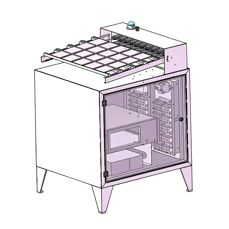
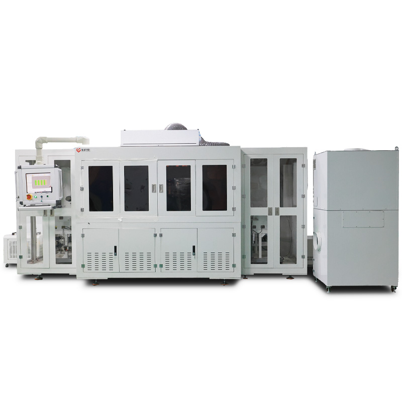
A production scribing tool is judged on: placement accuracy across the full plate (thermal drift compensation), throughput per step at target overlap, debris extraction (redeposition kills fill factor), inline vision metrology of scribe width and position, and recipe repeatability across shifts. Integrated platforms combining P1-P3, edge deletion and marking reduce handling and alignment losses between steps.
6. Working with Lecheng
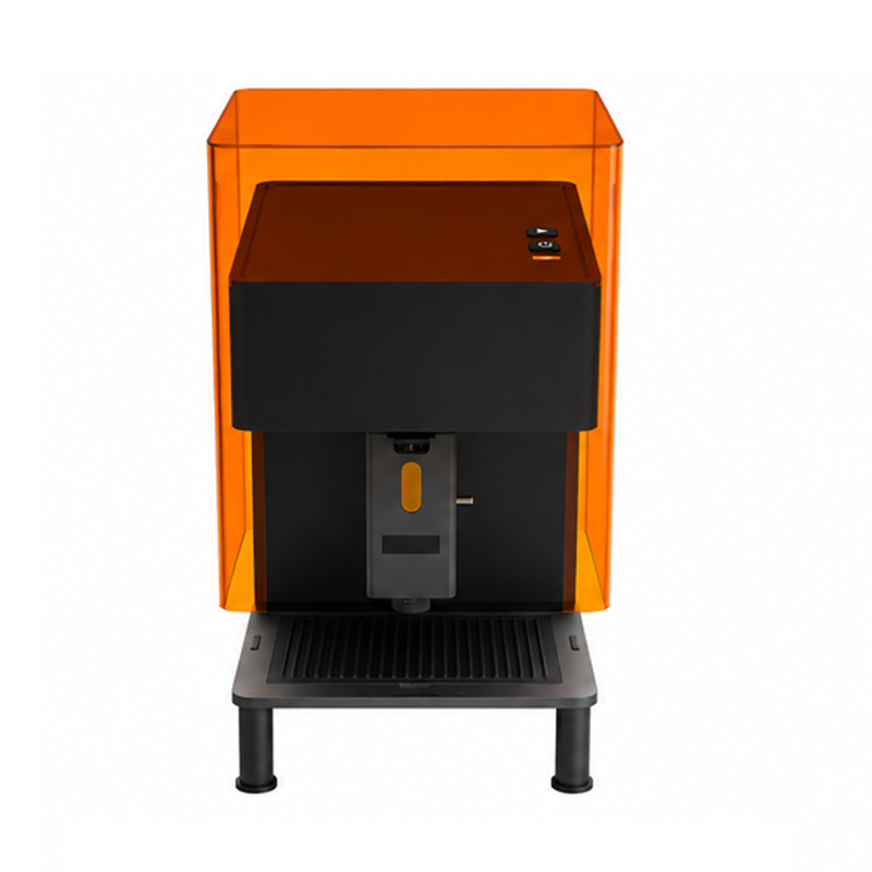
Lecheng builds laser scribing, edge isolation and integrated processing equipment for perovskite and thin-film photovoltaic lines, plus the marking, cutting and welding tools around them. Send us your layer stack, plate size and target takt: we run scribe trials on your samples, return SEM/microscope evidence of the P1-P3 quality, and propose a line configuration with metrology included.